Wesley L. Harris’s life is a testament to the power of mentorship and determination. Harris, born in 1941 in Richmond, Virginia, grew up during the tumultuous years of the Civil Rights Movement and faced an environment fraught with challenges. His parents, both of whom only had a third-grade education, walked to Richmond from rural Virginia counties when the Great Depression left the region’s farming communities destitute. They found work as laborers in the city’s tobacco factories but pushed their son to pursue higher education so he could live a better life.
Today, Harris is a professor of aeronautics and astronautics at MIT and heads the school’s Hypersonic Research Laboratory. More importantly, he is committed to fostering the next generation of engineers, particularly students of color.
“I’ve been keeping my head down, working with students of color—especially at the Ph.D. level—to produce more scholars,” Harris says. “I do feel good about that.”
From physics to aerospace engineering
Harris’s journey into the world of science began under the guidance of his physics teacher at the all-Black Armstrong High School, in Richmond. The instructor taught Harris how to build a cloud chamber to investigate the collision of alpha particles with water droplets. The chamber made it possible to visualize the passage of ionizing radiation emitted by radium 226, which Harris sourced from a wristwatch that used the substance to make the watch hands glow in the dark.
The project won first prize at Virginia’s statewide Black high school science fair, and he took the bold step of signing up for a separate science fair held for the state’s White students. Harris’s project received the third-place prize in physics at that event.
Those awards and his teacher’s unwavering belief in Harris’s potential pushed him to aim higher. He says that he wanted nothing more than to become a physicist like her. Ironically, it was also her influence that led him to shift his career path from physics to aeronautical engineering.
When discussing which college he should attend, she spoke to him as though he were a soldier getting his marching orders. “Wesley, you will go to the University of Virginia [in Charlottesville],” she proclaimed.
Harris applied, knowing full well that the school did not allow Black students in the 1960s to pursue degrees in mathematics, physics, chemistry, English, economics, or political science.
The only available point of entry for him was the university’s School of Engineering. He chose aerospace as his focus—the only engineering discipline that interested him. Harris became one of only seven Black students on a campus with 4,000 undergrads and the first Black student to join the prestigious Jefferson Society literary and debate club. He graduated in 1964 with a bachelor’s degree in aerospace engineering. He went on to earn his master’s and doctoral degrees in aerospace engineering from Princeton in 1966 and 1968, respectively.
Harris’s Ph.D. thesis advisor at Princeton reinforced the values of mentorship and leadership instilled by his high school teacher, urging Harris to focus not only on his research but on how he could uplift others.
Harris began his teaching career by breaking down barriers at the University of Virginia in 1968. He was the first Black person in the school’s history to be offered a tenured faculty position. He was also the university’s first Black engineering professor. In 1972, he joined MIT as a professor of aeronautics and astronautics.
Harris’s dedication to supporting underrepresented minority groups at MIT began early in his tenure. In 1975, he founded the Office of Minority Education, where he pioneered innovative teaching methods such as videotaping and replaying lectures, which helped countless students succeed. “Some of those old videotapes may still be around,” he says, laughing.
“I’ve been keeping my head down, working with students of color—especially at the Ph.D. level—to produce more scholars. I do feel good about that.”
Over the years, he has periodically stepped away from MIT to take on other roles, including Program Manager in the Fluid and Thermal Physics Office and as manager of Computational Methods at NASA’s headquarters in Washington, D.C., from 1979 to 1980. He returned to NASA in 1993 and served as Associate Administrator for Aeronautics, overseeing personnel, programs, and facilities until 1995.
Harris is a respected aeronautical innovator. Near the end of the Vietnam War, the U.S. Army approached MIT to help it solve a problem. Helicopters were being shot down by the enemy, who had learned to distinguish attack helicopters from those used for performing reconnaissance or transporting personnel and cargo by the noise they made. The Army needed a solution that would reduce the helicopters’ acoustic signatures without compromising performance. Harris and his aeronautics team at MIT delivered that technology. In January 1978, they presented a lab report detailing their findings to the U.S. Department of Defense. “Experimental and Theoretical Studies on Model Helicopter Rotor Noise” was subsequently published in The Journal of Sound and Vibration. A year later, Harris and his colleagues at the Fluid Dynamic Research Laboratory wrote another lab report on the topic, “Parametric Studies of Model Helicopter Blade Slap and Rotational Noise.”
Harris has also heightened scientists’ understanding of the climate-altering effects of shock waves propagating upward from aircraft flying at supersonic speeds. He discovered that these high-speed airflows trigger chemical reactions among the carbon, oxides, nitrides, and sulfides in the atmosphere.
Despite his technical achievements, Harris says his greatest fulfillment comes from mentoring students. He takes immense pride in the four students who recently earned doctorates in hypersonics under his guidance, especially a Black woman who graduated this year.
Harris’s commitment to nurturing young talent extends beyond his graduate students. For more than two decades, he has served as a housemaster at MIT’s New House residence hall, where he helps first-year undergraduate students successfully transition to campus life.
“You must provide an environment that fosters the total development of the student, not just mastery of physics, chemistry, math, and economics,” Harris says.
He takes great satisfaction in watching his students grow and succeed, knowing that he helped prepare them to make a positive impact on the world.
Reflecting on his career, Harris acknowledges the profound impact of the mentors who guided him. Their lessons continue to influence his work and his unwavering commitment to mentoring the next generation.
“I’ve always wanted to be like my high school teacher—a physicist who not only had deep knowledge of the scientific fundamentals but also compassion and love for Black folks,” he says.
Through his work, Harris has not only advanced the field of aerospace engineering but has also paved the way for future generations to soar.
Four decades after the first IEEE International Conference on Robotics and Automation (ICRA) in Atlanta, robotics is bigger than ever. Next week in Rotterdam is the IEEE ICRA@40 conference, “a celebration of 40 years of pioneering research and technological advancements in robotics and automation.” There’s an ICRA every year, of course. Arguably the largest robotics research conference in the world, the 2024 edition was held in Yokohama, Japan back in May.
ICRA@40 is not just a second ICRA conference in 2024. Next week’s conference is a single track that promises “a journey through the evolution of robotics and automation,” through four days of short keynotes from prominent roboticists from across the entire field. You can see for yourself, the speaker list is nuts. There are also debates and panels tackling big ideas, like: “What progress has been made in different areas of robotics and automation over the past decades, and what key challenges remain?” Personally, I’d say “lots” and “most of them,” but that’s probably why I’m not going to be up on stage.
Forty years ago is a long time, but it’s not that long, so just for fun, I had a look at the proceedings of ICRA 1984 which are available on IEEE Xplore, if you’re curious. Here’s an excerpt of the forward from the organizers, which included folks from International Business Machines and Bell Labs:
The proceedings of the first IEEE Computer Society International Conference on Robotics contains papers covering practically all aspects of robotics. The response to our call for papers has been overwhelming, and the number of papers submitted by authors outside the United States indicates the strong international interest in robotics. The Conference program includes papers on: computer vision; touch and other local sensing; manipulator kinematics, dynamics, control and simulation; robot programming languages, operating systems, representation, planning, man-machine interfaces; multiple and mobile robot systems. The technical level of the Conference is high with papers being presented by leading researchers in robotics. We believe that this conference, the first of a series to be sponsored by the IEEE, will provide a forum for the dissemination of fundamental research results in this fast developing field.
Technically, this was “ICR,” not “ICRA,” and it was put on by the IEEE Computer Society’s Technical Committee on Robotics, since there was no IEEE Robotics and Automation Society at that time; RAS didn’t get off the ground until 1987.
1984 ICR(A) had two tracks, and featured about 75 papers presented over three days. Looking through the proceedings, you’ll find lots of familiar names: Harry Asada, Ruzena Bajcsy, Ken Salisbury, Paolo Dario, Matt Mason, Toshio Fukuda, Ron Fearing, and Marc Raibert. Many of these folks will be at ICRA@40, so if you see them, make sure and thank them for helping to start it all, because 40 years of robotics is definitely something to celebrate.
Since 5G began its rollout in 2018 or 2019, fifth-generation wireless networks have spread across the globe to cover hundreds of millions of users. But while it offers lower latency than precursor networks, 5G also requires more base stations. To avoid installing unsightly equipment on more and more shared spaces, Japanese companies are developing transparent glass antennas that allow windows to serve as base stations that can be shared by several carriers.
Because 5G networks include spectrum comprising higher frequencies than 4G, base stations for 5G networks serve a smaller coverage footprint. Which means more base stations are needed compared to 4G. Due to a lack of installation spots and the high cost of rolling out 5G networks, carriers in Japan have been sharing mobile infrastructure.
Last month the Tokyo-based communications company JTower announced the deployment of the new glass antenna, created in part by glassmaker AGC (one of the world’s largest) and the mobile carrier NTT Docomo. The first was installed on a window in Tokyo’s Shinjuku district.
The product is “the world’s first antenna that turns a window into a base station that can be attached to a building window inside and turn the outdoors into a service area without spoiling the cityscape or the exterior appearance of the building,” says Shota Ochiai, a marketing manager at AGC.
NTT Docomo reports that it uses transparent conductive materials as the basis for its antenna, sandwiching the conductive material along with a transparent resin, the kind used in laminated windshields, in between two sheets of glass.
“I don’t think the idea for using transparent conductive materials as an antenna existed before,” said AGC’s Kentaro Oka in a company statement. “The durability of the antenna was significantly increased by placing the conductive materials between glass.”
The transparent antenna can be engineered according to the thickness of the glass to reduce the attenuation and reflection of the radio signals being absorbed and emitted by the window-sized device. “The glass antenna uses our proprietary technology to smooth out the disruption in the direction of radio waves when they pass through a window,” says Ochia.
A brief history of the window antenna
Branded WAVEANTENNA, the antenna is installed on the interior surface of windows. Apart perhaps from its cabling, the WAVEANTENNA is an otherwise inconspicuous piece of equipment that is often tucked out of sight, placed near the top or otherwise at the edges of a window.
It is compatible with frequencies in the 5G Sub6 band—meaning signals that are less than 6 gigahertz (GHz). Sub6 antennas represent critical portions of a 5G deployment, as their lower frequency ranges penetrate barriers like walls and buildings better than the substantially higher-bandwidth millimeter-wave portions of the 5G spectrum.
An earlier version of the product was launched in 2020, while a version that could handle sharing by multiple cell networks was introduced last year, according to AGC. The company says its antenna is optimized for frequencies between 3.7 and 4.5 GHz bands, which still allows for substantial bandwidth—albeit not comparable with what an ideal millimeter-wave 5G deployment could reach. (Millimeter waves can deliver typically between 10 and 50 GHz of bandwidth.)
The glass antenna can help expand 5G coverage as infrastructure sharing will become more important to carriers, AGC says. Besides increasing the number of locations for base stations, the device makes it easier to select the appropriate installation height, according to Ochiai.
AGC has also applied 5G glass antennas to automobiles, where they can help reduce dropped signals. The company reports that users include Halo.Car, an on-demand EV rental service in Las Vegas that relies on high-speed networks for remote drivers to deliver cars to customers.
More than 15 percent of the world’s population—greater than 1 billion people—live with disabilities including hearing loss, vision problems, mental health challenges, and lack of mobility. EPICS in IEEE has engaged students’ ingenuity worldwide to address accessibility issues through adaptive services, redesigned technology, and new assistive technologies during its 2023 Access and Abilities Competition.
The competition challenged university students around the world to use their engineering skills to help with accessibility issues. The EPICS in IEEE Committee received 58 proposals and selected 23 projects, which were funded in early 2023.
EPICS is a grant-based program for IEEE Educational Activities that funds service learning projects for university and high school students.
The teams, which include faculty members and IEEE members, create and execute engineering projects in partnership with organizations to improve their communities.
“Some gamers with arm or hand deficiencies play with their feet, nose, mouth, or elbows, or they use devices not intended for that purpose and are forced to adapt. I realized that if there was a dedicated device designed for such individuals, they’d be able to play and experience the joy of gaming.” —John McCauley.
The four EPICS in IEEE pillars are access and abilities; environment; education and outreach; and human services. In the Access and Abilities Competition, student teams received between US $1,000 and $10,000. Each team had 12 months to build a prototype or solution in collaboration with its community partners. The projects, which involved more than 350 students and 149 IEEE volunteers, aimed to help an estimated 8,000 people in the first year of deployment.
The teams included participants from IEEE student branches, IEEE Women in Engineering groups, IEEE–Eta Kappa Nu honor society chapters, and IEEE sections.
The competition was funded by the Taenzer Memorial Fund in 2019, with $90,000 allocated by the IEEE Foundation. The fund was established with a bequest from the estate of Jon C. Taenzer, an IEEE life senior member.
The student teams submitted their final reports this year.
Here are highlights from four of the projects:
Adaptive mouse for gaming
Members of the adaptive mouse EPICS in IEEE team at the University of Florida in Gainesville designed a device that contains keyboard functions and can be used with just one hand.EPICS in IEEE
A team of 10 biomedical engineering students at the University of Florida in Gainesville designed their project to help people whose hands or arms have an abnormality, so they could more easily play games.
The team built five adaptive mouse devices and plans to deliver them this year to five recipients involved with Hands to Love, a Florida-based organization that supports children with upper limb abnormalities.
The team incorporated the keyboard elements of gaming into a mouse, allowing gaming gestures and movements with just one hand. The 3D-printed mouse combines existing gaming technology, including the internal mechanisms of keyboards, a Logitech mouse, and Microsoft Xbox controller emulations. It allows the player to move and aim while gaming with just a mouse.
Gaming enthusiast John McCauley, a junior in the university’s biomedical engineering program, was behind the project’s conception.
“Some gamers with arm or hand deficiencies play with their feet, nose, mouth, or elbows, or they use devices not intended for that purpose and are forced to adapt,” McCauley says. “I realized that if there was a dedicated device designed for such individuals, they’d be able to play and experience the joy of gaming.”
The team used its $1,000 EPICS in IEEE grant to purchase the prototype’s components.
Making campus more accessible
Universidad Tecnólogica de Panamá students test their microcontroller-based prototype, designed to help make their school more accessible.EPICS in IEEE
A team of 15 undergraduate students from the Universidad Tecnológica de Panamá in Panama City and 24 students from four high schools in Chiriquí, Panama, created several projects focused on people with visual or physical disabilities. The team’s goal was to make their campus and community more accessible to those with different abilities. The projects enhanced their classmates’ autonomy and improved their quality of life.
The team made braille signs using a 3D printer, and they designed and built a personalized wheelchair. The students also automated the doors within the engineering department to provide better access to classrooms and corridors for those with disabilities.
“This project will be very useful, especially [in Panama], where buildings have not been adapted for people with disabilities,” said team member Gael Villarreal, a high school junior.
While working together on the project, team members honed their technical and interpersonal skills. They came to appreciate the importance of collaboration and communication.
“I learned that you need to have new experiences, be sociable, meet and get along with new people, and work as a team to be successful,” high school junior Gianny Rodriguez said.
The team used its $8,100 EPICS grant to purchase materials and train the community on using the new tools.
Helping children with hearing impairments
A team of students from the SRM Institute of Science and Technology student branch, in Chennai, India, worked with the Dr. MGR Home and Higher Secondary School for the Speech and Hearing Impaired, also in Chennai, to build a device to help children with hearing aids and cochlear implants learn Tamil, the local language. In rural areas, young children often do not have access to specialized speech and hearing health care providers to learn critical language skills. The team’s assistive device supports native language skill development, helping parents and trainers support the children in language and sound acquisition.
The project is designed to provide access to aural rehabilitation, including identifying hearing loss and therapies for children far from hospitals and rehabilitation centers.
The kiosklike device resembles an ATM and includes surround-sound speakers and touchscreens. It uses a touch monitor and microphones to access tasks and tests that help young children learn Tamil.
The team worked with 150 pupils at the school between the ages of 5 and 8 to develop the prototype. The built-in app includes tasks that focus on improving auditory awareness, auditory discrimination (the ability to recognize, compare, and distinguish between distinct sounds), and language acquisition (how people perceive and comprehend language).
The device tests the pupil’s hearing range based on sounds with visual cues, sounds at low intensity, sounds in the presence of noise, and sound direction.
The speakers emulate real-life situations and are used to relay the teacher’s instructions.
The team received a $1,605 grant to execute the project.
This video spotlights the challenges youngsters with hearing disabilities in Chenni, India, face and how the assistive technology will help them.
Self-navigating robotic walking aid
Students from the IEEE Swinburne Sarawak student branch in Malaysia brought a prototype of their walking aid to Trinity Eldercare, their community partner.EPICS in IEEE
The team wanted to improve existing walkers on the market, so they surveyed residents at Trinity Eldercare to find out what features would be useful to them.
The students’ prototype, based on a commercial walker, includes a wearable haptic belt that detects obstacles and alerts the user. Pressure sensors in the hand grips sense which direction the user wants to go. One of the senior citizens’ most requested features was the ability to locate a misplaced walker. The team was able to address the issue using sensors.
“I gained substantial knowledge in robotics programming and artificial intelligence and deep learning integration for person tracking and autonomous navigation,” one of the team members said. “Additionally, presenting our smart walker prototype at the International Invention, Innovation, Technolgy Competition and Exhibition in Malaysia enhanced my presentation skills, as I successfully articulated its viability and usefulness to the judges.”
The project received a $1,900 grant.
Join the EPICS in IEEE mailing list to learn more about all the Access and Abilities Competition projects and other impactful efforts made possible by donations to the IEEE Foundation. To learn more, check out the video of the competition:
The EPICS in IEEE program is celebrating its 15th year of supporting and facilitating service-learning projects and impacting students and communities worldwide
Maybe you’ve read about Gary Marcus’s testimony before the Senate in May of 2023, when he sat next to Sam Altman and called for strict regulation of Altman’s company, OpenAI, as well as the other tech companies that were suddenly all-in on generative AI. Maybe you’ve caught some of his arguments on Twitter with Geoffrey Hinton and Yann LeCun, two of the so-called “godfathers of AI.” One way or another, most people who are paying attention to artificial intelligence today know Gary Marcus’s name, and know that he is not happy with the current state of AI.
He lays out his concerns in full in his new book, Taming Silicon Valley: How We Can Ensure That AI Works for Us, which was published today by MIT Press. Marcus goes through the immediate dangers posed by generative AI, which include things like mass-produced disinformation, the easy creation of deepfake pornography, and the theft of creative intellectual property to train new models (he doesn’t include an AI apocalypse as a danger, he’s not a doomer). He also takes issue with how Silicon Valley has manipulated public opinion and government policy, and explains his ideas for regulating AI companies.
Marcus studied cognitive science under the legendary Steven Pinker, was a professor at New York University for many years, and co-founded two AI companies, Geometric Intelligence and Robust.AI. He spoke with IEEE Spectrum about his path to this point.
What was your first introduction to AI?
Gary MarcusBen Wong
Gary Marcus: Well, I started coding when I was eight years old. One of the reasons I was able to skip the last two years of high school was because I wrote a Latin-to-English translator in the programming language Logo on my Commodore 64. So I was already, by the time I was 16, in college and working on AI and cognitive science.
So you were already interested in AI, but you studied cognitive science both in undergrad and for your Ph.D. at MIT.
Marcus: Part of why I went into cognitive science is I thought maybe if I understood how people think, it might lead to new approaches to AI. I suspect we need to take a broad view of how the human mind works if we’re to build really advanced AI. As a scientist and a philosopher, I would say it’s still unknown how we will build artificial general intelligence or even just trustworthy general AI. But we have not been able to do that with these big statistical models, and we have given them a huge chance. There’s basically been $75 billion spent on generative AI, another $100 billion on driverless cars. And neither of them has really yielded stable AI that we can trust. We don’t know for sure what we need to do, but we have very good reason to think that merely scaling things up will not work. The current approach keeps coming up against the same problems over and over again.
What do you see as the main problems it keeps coming up against?
Marcus: Number one is hallucinations. These systems smear together a lot of words, and they come up with things that are true sometimes and not others. Like saying that I have a pet chicken named Henrietta is just not true. And they do this a lot. We’ve seen this play out, for example, in lawyers writing briefs with made-up cases.
Second, their reasoning is very poor. My favorite examples lately are these river-crossing word problems where you have a man and a cabbage and a wolf and a goat that have to get across. The system has a lot of memorized examples, but it doesn’t really understand what’s going on. If you give it a simpler problem, like one Doug Hofstadter sent to me, like: “A man and a woman have a boat and want to get across the river. What do they do?” It comes up with this crazy solution where the man goes across the river, leaves the boat there, swims back, something or other happens.
Sometimes he brings a cabbage along, just for fun.
Marcus: So those are boneheaded errors of reasoning where there’s something obviously amiss. Every time we point these errors out somebody says, “Yeah, but we’ll get more data. We’ll get it fixed.” Well, I’ve been hearing that for almost 30 years. And although there is some progress, the core problems have not changed.
Let’s go back to 2014 when you founded your first AI company, Geometric Intelligence. At that time, I imagine you were feeling more bullish on AI?
Marcus: Yeah, I was a lot more bullish. I was not only more bullish on the technical side. I was also more bullish about people using AI for good. AI used to feel like a small research community of people that really wanted to help the world.
So when did the disillusionment and doubt creep in?
Marcus: In 2018 I already thought deep learning was getting overhyped. That year I wrote this piece called “Deep Learning, a Critical Appraisal,” which Yann LeCun really hated at the time. I already wasn’t happy with this approach and I didn’t think it was likely to succeed. But that’s not the same as being disillusioned, right?
Then when large language models became popular [around 2019], I immediately thought they were a bad idea. I just thought this is the wrong way to pursue AI from a philosophical and technical perspective. And it became clear that the media and some people in machine learning were getting seduced by hype. That bothered me. So I was writing pieces about GPT-3 [an early version of OpenAI's large language model] being a bullshit artist in 2020. As a scientist, I was pretty disappointed in the field at that point. And then things got much worse when ChatGPT came out in 2022, and most of the world lost all perspective. I began to get more and more concerned about misinformation and how large language models were going to potentiate that.
You’ve been concerned not just about the startups, but also the big entrenched tech companies that jumped on the generative AI bandwagon, right? Like Microsoft, which has partnered with OpenAI?
Marcus: The last straw that made me move from doing research in AI to working on policy was when it became clear that Microsoft was going to race ahead no matter what. That was very different from 2016 when they released [an early chatbot named] Tay. It was bad, they took it off the market 12 hours later, and then Brad Smith wrote a book about responsible AI and what they had learned. But by the end of the month of February 2023, it was clear that Microsoft had really changed how they were thinking about this. And then they had this ridiculous “Sparks of AGI” paper, which I think was the ultimate in hype. And they didn’t take down Sydney after the crazy Kevin Roose conversation where [the chatbot] Sydney told him to get a divorce and all this stuff. It just became clear to me that the mood and the values of Silicon Valley had really changed, and not in a good way.
I also became disillusioned with the U.S. government. I think the Biden administration did a good job with its executive order. But it became clear that the Senate was not going to take the action that it needed. I spoke at the Senate in May 2023. At the time, I felt like both parties recognized that we can’t just leave all this to self-regulation. And then I became disillusioned [with Congress] over the course of the last year, and that’s what led to writing this book.
You talk a lot about the risks inherent in today’s generative AI technology. But then you also say, “It doesn’t work very well.” Are those two views coherent?
Marcus: There was a headline: “Gary Marcus Used to Call AI Stupid, Now He Calls It Dangerous.” The implication was that those two things can’t coexist. But in fact, they do coexist. I still think gen AI is stupid, and certainly cannot be trusted or counted on. And yet it is dangerous. And some of the danger actually stems from its stupidity. So for example, it’s not well-grounded in the world, so it’s easy for a bad actor to manipulate it into saying all kinds of garbage. Now, there might be a future AI that might be dangerous for a different reason, because it’s so smart and wily that it outfoxes the humans. But that’s not the current state of affairs.
Marcus: Let’s clarify: I don’t think generative AI is going to disappear. For some purposes, it is a fine method. You want to build autocomplete, it is the best method ever invented. But there’s a financial bubble because people are valuing AI companies as if they’re going to solve artificial general intelligence. In my view, it’s not realistic. I don’t think we’re anywhere near AGI. So then you’re left with, “Okay, what can you do with generative AI?”
Last year, because Sam Altman was such a good salesman, everybody fantasized that we were about to have AGI and that you could use this tool in every aspect of every corporation. And a whole bunch of companies spent a bunch of money testing generative AI out on all kinds of different things. So they spent 2023 doing that. And then what you’ve seen in 2024 are reports where researchers go to the users of Microsoft’s Copilot—not the coding tool, but the more general AI tool—and they’re like, “Yeah, it doesn’t really work that well.” There’s been a lot of reviews like that this last year.
The reality is, right now, the gen AI companies are actually losing money. OpenAI had an operating loss of something like $5 billion last year. Maybe you can sell $2 billion worth of gen AI to people who are experimenting. But unless they adopt it on a permanent basis and pay you a lot more money, it’s not going to work. I started calling OpenAI the possible WeWork of AI after it was valued at $86 billion. The math just didn’t make sense to me.
What would it take to convince you that you’re wrong? What would be the head-spinning moment?
Marcus: Well, I’ve made a lot of different claims, and all of them could be wrong. On the technical side, if someone could get a pure large language model to not hallucinate and to reason reliably all the time, I would be wrong about that very core claim that I have made about how these things work. So that would be one way of refuting me. It hasn’t happened yet, but it’s at least logically possible.
On the financial side, I could easily be wrong. But the thing about bubbles is that they’re mostly a function of psychology. Do I think the market is rational? No. So even if the stuff doesn’t make money for the next five years, people could keep pouring money into it.
The place that I’d like to prove me wrong is the U.S. Senate. They could get their act together, right? I’m running around saying, “They’re not moving fast enough,” but I would love to be proven wrong on that. In the book, I have a list of the 12 biggest risks of generative AI. If the Senate passed something that actually addressed all 12, then my cynicism would have been mislaid. I would feel like I’d wasted a year writing the book, and I would be very, very happy.
It’s hard to overstate Nvidia’s AI dominance. Founded in 1993,
Nvidia first made its mark in the then-new field of graphics processing units (GPUs) for personal computers. But it’s the company’s AI chips, not PC graphics hardware, that vaulted Nvidia into the ranks of the world’s most valuable companies. It turns out that Nvidia’s GPUs are also excellent for AI. As a result, its stock is more than 15 times as valuable as it was at the start of 2020; revenues have ballooned from roughly US $12 billion in its 2019 fiscal year to $60 billion in 2024; and the AI powerhouse’s leading-edge chips are as scarce, and desired, as water in a desert.
Access to
GPUs “has become so much of a worry for AI researchers, that the researchers think about this on a day-to-day basis. Because otherwise they can’t have fun, even if they have the best model,” says Jennifer Prendki, head of AI data at Google DeepMind. Prendki is less reliant on Nvidia than most, as Google has its own homespun AI infrastructure. But other tech giants, like Microsoft and Amazon, are among Nvidia’s biggest customers, and continue to buy its GPUs as quickly as they’re produced. Exactly who gets them and why is the subject of an antitrust investigation by the U.S. Department of Justice, according to pressreports.
Nvidia’s AI dominance, like the explosion of machine learning itself, is a recent turn of events. But it’s rooted in the company’s decades-long effort to establish GPUs as general computing hardware that’s useful for many tasks besides rendering graphics. That effort spans not only the company’s GPU architecture, which evolved to include “tensor cores” adept at accelerating AI workloads, but also, critically, its software platform, called
Cuda, to help developers take advantage of the hardware.
“They made sure every computer-science major coming out of university is trained up and knows how to
program CUDA,” says Matt Kimball, principal data-center analyst at Moor Insights & Strategy. “They provide the tooling and the training, and they spend a lot of money on research.”
Released in 2006, CUDA helps developers use an Nvidia GPU’s many cores. That’s proved essential for accelerating highly parallelized compute tasks, including modern generative AI. Nvidia’s success in building the CUDA ecosystem makes its hardware the path of least resistance for AI development. Nvidia chips might be in short supply, but the only thing more difficult to find than AI hardware is experienced AI developers—and many are familiar with CUDA.
That gives Nvidia a deep, broad moat with which to defend its business, but that doesn’t mean it lacks competitors ready to storm the castle, and their tactics vary widely. While decades-old companies like
Advanced Micro Devices (AMD) and Intel are looking to use their own GPUs to rival Nvidia, upstarts like Cerebras and SambaNova have developed radical chip architectures that drastically improve the efficiency of generative AI training and inference. These are the competitors most likely to challenge Nvidia.
Nvidia’s Armory
While Nvidia has several types of GPUs deployed, the big guns found in data centers are the H100 and H200. As soon as the end of 2024, they will be joined by the B200, which nearly quadruples the H100’s performance on a per-GPU basis.Sources: Nvidia, MLPerf inferencing v4.1 results for Llama2-70B
AMD: The other GPU maker
Pro: AMD GPUs are convincing Nvidia alternatives
Con: Software ecosystem can’t rival Nvidia’s CUDA
AMD has battled Nvidia in the graphics-chip arena for nearly two decades. It’s been, at times, a lopsided fight. When it comes to graphics, AMD’s GPUs have rarely beaten Nvidia’s in sales or mindshare. Still, AMD’s hardware has its strengths. The company’s broad GPU portfolio extends from integrated graphics for laptops to AI-focused data-center GPUs with over 150 billion transistors. The company was also an early supporter and adopter of
high-bandwidth memory (HBM), a form of memory that’s now essential to the world’s most advanced GPUs.
“If you look at the hardware…it stacks up favorably” to Nvidia, says Kimball, referring to AMD’s Instinct MI325X, a competitor of Nvidia’s H100. “AMD did a fantastic job laying that chip out.”
The MI325X, slated to launch by the end of the year, has over 150 billion transistors and 288 gigabytes of high-bandwidth memory, though real-world results remain to be seen. The MI325X’s predecessor, the
MI300X, earned praise from Microsoft, which deploys AMD hardware, including the MI300X, to handle some ChatGPT 3.5 and 4 services. Meta and Dell have also deployed the MI300X, and Meta used the chips in parts of the development of its latest large language model, Llama 3.1.
There’s still a hurdle for AMD to leap: software. AMD offers an open-source platform,
ROCm, to help developers program its GPUs, but it’s less popular than CUDA. AMD is aware of this weakness, and in July 2024, it agreed to buy Europe’s largest private AI lab, Silo AI, which has experience doing large-scale AI training using ROCm and AMD hardware. AMD has also plans to purchase ZT Systems, a company with expertise in data-center infrastructure, to help the company serve customers looking to deploy its hardware at scale. Building a rival to CUDA is no small feat, but AMD is certainly trying.
Con: Next big AI chip doesn’t arrive until late 2025
Intel’s challenge is the opposite of AMD’s.
While Intel lacks an exact match for Nvidia’s CUDA and AMD’s ROCm, it launched an open-source unified programming platform,
OneAPI, in 2018. Unlike CUDA and ROCm, OneAPI spans multiple categories of hardware, including CPUs, GPUs, and FPGAs. So it can help developers accelerate AI tasks (and many others) on any Intel hardware. “Intel’s got a heck of a software ecosystem it can turn on pretty easily,” says Kimball.
Hardware, on the other hand, is a weakness, at least when compared to Nvidia and AMD. Intel’s Gaudi AI accelerators, the fruit of Intel’s
2019 acquisition of AI hardware startup Habana Labs, have made headway, and the latest, Gaudi 3, offers performance that’s competitive with Nvidia’s H100.
However, it’s unclear precisely what Intel’s next hardware release will look like, which has caused some concern. “Gaudi 3 is very capable,” says
Patrick Moorhead, founder of Moor Insights & Strategy. But as of July 2024 “there is no Gaudi 4,” he says.
Intel instead plans to pivot to an ambitious chip, code-named Falcon Shores, with a tile-based modular architecture that combines Intel
x86 CPU cores and Xe GPU cores; the latter are part of Intel’s recent push into graphics hardware. Intel has yet to reveal details about Falcon Shores’ architecture and performance, though, and it’s not slated for release until late 2025.
Cerebras: Bigger is better
Pro: Wafer-scale chips offer strong performance and memory per chip
Con: Applications are niche due to size and cost
Make no mistake: AMD and Intel are by far the most credible challengers to Nvidia. They share a history of designing successful chips and building programming platforms to go alongside them. But among the smaller, less proven players, one stands out:
Cerebras.
The company, which specializes in AI for supercomputers, made waves in 2019 with the Wafer Scale Engine, a gigantic, wafer-size piece of silicon packed with 1.2 trillion transistors. The most recent iteration, Wafer Scale Engine 3, ups the ante to 4 trillion transistors. For comparison, Nvidia’s largest and newest GPU, the
B200, has “just” 208 billion transistors. The computer built around this wafer-scale monster, Cerebras’s CS-3, is at the heart of the Condor Galaxy 3, which will be an 8-exaflop AI supercomputer made up of 64 CS-3s. G42, an Abu Dhabi–based conglomerate that hopes to train tomorrow’s leading-edge large language models, will own the system.
“It’s a little more niche, not as general purpose,” says
Stacy Rasgon, senior analyst at Bernstein Research. “Not everyone is going to buy [these computers]. But they’ve got customers, like the [United States] Department of Defense, and [the Condor Galaxy 3] supercomputer.”
Cerebras’s WSC-3 isn’t going to challenge Nvidia, AMD, or Intel hardware in most situations; it’s too large, too costly, and too specialized. But it could give Cerebras a unique edge in supercomputers, because no other company designs chips on the scale of the WSE.
SambaNova: A transformer for transformers
Pro: Configurable architecture helps developers squeeze efficiency from AI models
Con: Hardware still has to prove relevance to mass market
SambaNova, founded in 2017, is another chip-design company tackling AI training with an unconventional chip architecture. Its flagship, the SN40L, has what the company calls a “reconfigurable dataflow architecture” composed of tiles of memory and compute resources. The links between these tiles can be altered on the fly to facilitate the quick movement of data for large neural networks.
Prendki believes such customizable silicon could prove useful for training large language models, because AI developers can optimize the hardware for different models. No other company offers that capability, she says.
SambaNova is also scoring wins with
SambaFlow, the software stack used alongside the SN40L. “At the infrastructure level, SambaNova is doing a good job with the platform,” says Moorhead. SambaFlow can analyze machine learning models and help developers reconfigure the SN40L to accelerate the model’s performance. SambaNova still has a lot to prove, but its customers include SoftBank and Analog Devices.
Groq: Form for function
Pro: Excellent AI inference performance
Con: Application currently limited to inference
Yet another company with a unique spin on AI hardware is
Groq. Groq’s approach is focused on tightly pairing memory and compute resources to accelerate the speed with which a large language model can respond to prompts.
“Their architecture is very memory based. The memory is tightly coupled to the processor. You need more nodes, but the price per token and the performance is nuts,” says Moorhead. The “token” is the basic unit of data a model processes; in an LLM, it’s typically a word or portion of a word. Groq’s performance is even more impressive, he says, given that its chip, called the
Language Processing Unit Inference Engine, is made using GlobalFoundries’ 14-nanometer technology, several generations behind the TSMC technology that makes the Nvidia H100.
In July, Groq posted a demonstration of its chip’s inference speed, which can exceed 1,250 tokens per second running
Meta’s Llama 3 8-billion parameter LLM. That beats even SambaNova’s demo, which can exceed 1,000 tokens per second.
Qualcomm: Power is everything
Pro: Broad range of chips with AI capabilities
Con: Lacks large, leading-edge chips for AI training
Qualcomm, well known for the Snapdragon system-on-a-chip that powers popular Android phones like the Samsung Galaxy S24 Ultra and OnePlus 12, is a giant that can stand toe-to-toe with AMD, Intel, and Nvidia.
But unlike those peers, the company is focusing its AI strategy more on AI inference and energy efficiency for specific tasks.
Anton Lokhmotov, a founding member of the AI benchmarking organization MLCommons and CEO of Krai, a company that specializes in AI optimization, says Qualcomm has significantly improved the inference of the Qualcomm Cloud AI 100 servers in an important benchmark test. The servers’ performance increased from 180 to 240 samples-per-watt in ResNet-50, an image-classification benchmark, using “essentially the same server hardware,” Lokhmotov notes.
Efficient AI inference is also a boon on devices that need to handle AI tasks locally without reaching out to the cloud, says Lokhmotov. Case in point: Microsoft’s
Copilot Plus PCs. Microsoft and Qualcomm partnered with laptop makers, including Dell, HP, and Lenovo, and the first Copilot Plus laptops with Qualcomm chips hit store shelves in July. Qualcomm also has a strong presence in smartphones and tablets, where its Snapdragon chips power devices from Samsung, OnePlus, and Motorola, among others.
Qualcomm is an important player in AI for driver assist and self-driving platforms, too. In early 2024, Hyundai’s Mobius division announced a partnership to use the
Snapdragon Ride platform, a rival to Nvidia’s Drive platform, for advanced driver-assist systems.
The Hyperscalers: Custom brains for brawn
Pros: Vertical integration focuses design
Cons: Hyperscalers may prioritize their own needs and uses first
Hyperscalers—cloud-computing giants that deploy hardware at vast scales—are synonymous with Big Tech. Amazon, Apple, Google, Meta, and Microsoft all want to deploy AI hardware as quickly as possible, both for their own use and for their cloud-computing customers. To accelerate that, they’re all designing chips in-house.
Google began investing in AI processors much earlier than its competitors: The search giant’s Tensor Processing Units, first announced in 2015, now power most of its AI infrastructure. The sixth generation of TPUs,
Trillium, was announced in May and is part of Google’s AI Hypercomputer, a cloud-based service for companies looking to handle AI tasks.
Prendki says Google’s TPUs give the company an advantage in pursuing AI opportunities. “I’m lucky that I don’t have to think too hard about where I get my chips,” she says. Access to TPUs doesn’t entirely eliminate the supply crunch, though, as different Google divisions still need to share resources.
And Google is no longer alone. Amazon has two in-house chips,
Trainium and Inferentia, for training and inference, respectively. Microsoft has Maia, Meta has MTIA, and Apple is supposedly developing silicon to handle AI tasks in its cloud infrastructure.
None of these compete directly with Nvidia, as hyperscalers don’t sell hardware to customers. But they do sell access to their hardware through cloud services, like
Google’s AI Hypercomputer, Amazon’s AWS, and Microsoft’s Azure. In many cases, hyperscalers offer services running on their own in-house hardware as an option right alongside services running on hardware from Nvidia, AMD, and Intel; Microsoft is thought to be Nvidia’s largest customer.
David Plunkert
Chinese chips: An opaque future
Another category of competitor is born not of technical needs but of geopolitical realities.
The United States has imposed restrictions on the export of AI hardware that prevents chipmakers from selling their latest, most-capable chips to Chinese companies. In response, Chinese companies are designing homegrown AI chips.
Huawei is a leader. The company’s
Ascend 910B AI accelerator, designed as an alternative to Nvidia’s H100, is in production at Semiconductor Manufacturing International Corp., a Shanghai-based foundry partially owned by the Chinese government. However, yield issues at SMIC have reportedly constrained supply. Huawei is also selling an “AI-in-a-box” solution, meant for Chinese companies looking to build their own AI infrastructure on-premises.
To get around the U.S. export control rules, Chinese industry could turn to alternative technologies. For example, Chinese researchers have made headway in photonic chips that use light, instead of electric charge, to perform calculations. “The advantage of a beam of light is you can cross one [beam with] another,” says Prendki. “So it reduces constraints you’d normally have on a silicon chip, where you can’t cross paths. You can make the circuits more complex, for less money.” It’s still very early days for photonic chips, but Chinese investment in the area could accelerate its development.
Room for more
It’s clear that Nvidia has no shortage of competitors. It’s equally clear that none of them will challenge—never mind defeat—Nvidia in the next few years. Everyone interviewed for this article agreed that Nvidia’s dominance is currently unparalleled, but that doesn’t mean it will crowd out competitors forever.
“Listen, the market wants choice,” says Moorhead. “I can’t imagine AMD not having 10 or 20 percent market share, Intel the same, if we go to 2026. Typically, the market likes three, and there we have three reasonable competitors.” Kimball says the hyperscalers, meanwhile, could challenge Nvidia as they transition more AI services to in-house hardware.
And then there’s the wild cards. Cerebras, SambaNova, and Groq are the leaders in a very long list of startups looking to nibble away at Nvidia with novel solutions. They’re joined by dozens of others, including
d-Matrix, Untether, Tenstorrent, and Etched, all pinning their hopes on new chip architectures optimized for generative AI. It’s likely many of these startups will falter, but perhaps the next Nvidia will emerge from the survivors.
Scottish inventor
John Logie Baird had a lot of ingenious ideas, not all of which caught on. His phonovision was an early attempt at video recording, with the signals preserved on phonograph records. His noctovision used infrared light to see objects in the dark, which some experts claim was a precursor to radar.
But Baird earned his spot in history with the televisor. On 26 January 1926, select members of the Royal Institution gathered at Baird’s lab in London’s Soho neighborhood to witness the broadcast of a small but clearly defined image of a ventriloquist dummy’s face, sent from the televisor’s electromechanical transmitter to its receiver. He also demonstrated the televisor with a human subject, who observers could see speaking and moving on the screen. For this, Baird is often credited with the first public demonstration of television.
John Logie Baird [shown here] used the heads of ventriloquist dummies in early experiments because they didn’t mind the heat and bright lights of his televisor. Science History Images/Alamy
How the Nipkow Disk Led to Baird’s Televisor
To be clear, Baird didn’t invent television. Television is one of those inventions that benefited from many contributors, collaborators, and competitors. Baird’s starting point was an idea for an “electric telescope,” patented in 1885 by German engineer
Paul Nipkow.
Nipkow’s apparatus captured a picture by dividing it into a vertical sequence of lines, using a spinning disk with perforated holes around the edge. The perforations were offset in a spiral so that each hole captured one slice of the image in turn—known today as scan lines. Each line would be encoded as an electrical signal. A receiving apparatus converted the signals into light, to reconstruct the image. Nipkow never commercialized his electric telescope, though, and after 15 years the patent expired.
The inset on the left shows how the televisor split an image (in this case, a person’s face) into vertical lines. Bettmann/Getty Images
The system that Baird demonstrated in 1926 used two Nipkow disks, one in the transmitting apparatus and the other in the receiving apparatus. Each disk had 30 holes. He fitted the disk with glass lenses that focused the reflected light onto a photoelectric cell. As the transmitting disk rotated, the photoelectric cell detected the change in brightness coming through the individual lenses and converted the light into an electrical signal.
This signal was then sent to the receiving system. (Part of the receiving apparatus,
housed at the Science Museum in London, is shown at top.) There the process was reversed, with the electrical signal first being amplified and then modulating a neon gas–discharge lamp. The light passed through a rectangular slot to focus it onto the receiving Nipkow disk, which was turning at the same speed as the transmitter. The image could be seen on a ground glass plate.
Early experiments used a dummy because the many incandescent lights needed to provide sufficient illumination made it too hot and bright for a person. Each hole in the disk captured only a small bit of the overall image, but as long as the disk spun fast enough, the brain could piece together the complete image, a phenomenon known as persistence of vision. (In a 2022 Hands On column, Markus Mierse explains how to build a
modern Nipkow-disk electromechanical TV using a 3D printer, an LED module, and an Arduino Mega microcontroller.)
John Logie Baird and “True Television”
Regular readers of
this column know the challenge of documenting historical “firsts”—the first radio, the first telegraph, the first high-tech prosthetic arm. Baird’s claim to the first public broadcast of television is no different. To complicate matters, the actual first demonstration of his televisor wasn’t on 26 January 1926 in front of those esteemed members of the Royal Institution; rather, it occurred in March 1925 in front of curious shoppers at a Selfridges department store.
As Donald F. McLean recounts in his excellent June 2022 article “Before ‘True Television’: Investigating John Logie Baird’s 1925 Original Television Apparatus,” Baird used a similar device for the Selfridges demo, but it had only 16 holes, organized as two groups of eight, hence its nickname the Double-8. The resolution was about as far from high definition as you could get, showing shadowy silhouettes in motion. Baird didn’t consider this “true television,” as McLean notes in his Proceedings of the IEEE piece.
In 1926, Baird loaned part of the televisor he used in his Selfridges demo to the Science Museum in London.PA Images/Getty Images
Writing in December 1926 in
Experimental Wireless & The Wireless Engineer, Baird defined true television as “the transmission of the image of an object with all gradations of light, shade, and detail, so that it is seen on the receiving screen as it appears to the eye of an actual observer.” Consider the Selfridges demo a beta test and the one for the Royal Institution the official unveiling. (In 2017, the IEEE chose to mark the latter and not the former with a Milestone.)
The 1926 demonstration was a turning point in Baird’s career. In 1927 he established the
Baird Television Development Co., and a year later he made the first transatlantic television transmission, from London to Hartsdale, N.Y. In 1929, the BBC decided to give Baird’s system a try, performing some experimental broadcasts outside of normal hours. After that, mechanical television took off in Great Britain and a few other European countries.
But Wait There’s More!
If you enjoyed this dip into the history of television, check out
Spectrum’s new video collaboration with the YouTube channel Asianometry, which will offer a variety of perspectives on fascinating chapters in the history of technology. The first set of videos looks at the commercialization of color television.
Head over to Asianometry to see how Sony finally conquered the challenges of mass production of color TV sets with its Trinitron line. On
Spectrum’s YouTube channel, you’ll find a video—written and narrated by yours truly—on how the eminent physicist Ernest O. Lawrence dabbled for a time in commercial TVs. Spoiler alert: Lawrence had much greater success with the cyclotron and government contracts than he ever did commercializing his Chromatron TV. Spectrum also has a video on the yearslong fight between CBS and RCA over the U.S. standard for color TV broadcasting. —A.M.
The BBC used various versions of Baird’s mechanical system from 1929 to 1937, starting with the 30-line system and upgrading to a 240-line system. But eventually the BBC switched to the all-electronic system developed by Marconi-EMI. Baird then switched to working on one of the earliest electronic
color television systems, called the Telechrome. (Baird had already demonstrated a successful mechanical color television system in 1928, but it never caught on.) Meanwhile, in the United States, Columbia Broadcasting System (CBS) attempted to develop a mechanical color television system based on Baird’s original idea of a color wheel but finally ceded to an electronic standard in 1953.
Baird also experimented with stereoscopic or three-dimensional television and a 1,000-line display, similar to today’s high-definition television. Unfortunately, he died in 1946 before he could persuade anyone to take up that technology.
In a
1969 interview in TV Times, John’s widow, Margaret Baird, reflected on some of the developments in television that would have made her husband happy. He would enjoy the massive amounts of sports coverage available, she said. (Baird had done the first live broadcast of the Epsom Derby in 1931.) He would be thrilled with current affairs programs. And, my personal favorite, she thought he would love the annual broadcasting of the Eurovision song contest.
Other TV Inventors: Philo Farnsworth, Vladimir Zworykin
But as I said, television is an invention that’s had many contributors. Across the Atlantic,
Philo Farnsworth was experimenting with an all-electrical system that he had first envisioned as a high school student in 1922. By 1926, Farnsworth had secured enough financial backing to work full time on his idea.
One of his main inventions was the image dissector, also known as a dissector tube. This video camera tube creates a temporary electron image that can be converted into an electrical signal. On 7 September 1927, Farnsworth and his team successfully transmitted a single black line, followed by other images of simple shapes. But the system could only handle silhouettes, not three-dimensional objects.
Meanwhile,
Vladimir Zworykin was also experimenting with electronic television. In 1923, he applied for a patent for a video tube called the iconoscope. But it wasn’t until 1931, after he joined RCA, that his team developed a working version, which suspiciously came after Zworykin visited Farnsworth’s lab in California. The iconoscope overcame some of the dissector tube’s deficiencies, especially the storage capacity. It was also more sensitive and easier to manufacture. But one major drawback of both the image dissector and the iconoscope was that, like Baird’s original televisor, they required very bright lights.
Everyone was working to develop a better tube, but Farnsworth claimed that he’d invented both the concept of an electronic image moving through a vacuum tube as well as the idea of a storage-type camera tube. The iconoscope and any future improvements all depended on these progenitor patents. RCA knew this and offered to buy Farnsworth’s patents, but Farnsworth refused to sell. A multiyear patent-interference case ensued, finally finding for Farnsworth in 1935.
While the case was being litigated, Farnsworth made the first public demonstration of an all-electric television system on 25 August 1934 at the Franklin Institute in Philadelphia. And in 1939, RCA finally agreed to pay royalties to Farnsworth to use his patented technologies. But Farnsworth was never able to compete commercially with RCA and its all-electric television system, which went on to dominate the U.S. television market.
Eventually, Harold Law, Paul Weimer, and Russell Law developed a better tube at their Princeton labs, the image orthicon. Designed for TV-guided missiles for the U.S. military, it was 100 to 1,000 times as sensitive as the iconoscope. After World War II, RCA quickly adopted the tube for its TV cameras. The image orthicon became the industry standard by 1947, remaining so until 1968 and the move to color TV.
The Path to Television Was Not Obvious
My Greek teacher hated the word “television.” He considered it an abomination that combined the Greek prefix
telos (far off) with a Latin base, videre (to see). But early television was a bit of an abomination—no one really knew what it was going to be. As Chris Horrocks lays out in his delightfully titled book, The Joy of Sets(2017), television was developed in relation to the media that came before—telegraph, telephone, radio, and film.
Was television going to be like a telegraph, with communication between two points and an image slowly reassembled? Was it going to be like a telephone, with direct and immediate dialog between both ends? Was it going to be like film, with prerecorded images played back to a wide audience? Or would it be more like radio, which at the time was largely live broadcasts? At the beginning, people didn’t even know they wanted a television; manufacturers had to
convince them.
And technically, there were many competing visions—Baird’s, Farnsworth’s, Zworykin’s, and others. It’s no wonder that television took many years, with lots of false starts and dead ends, before it finally took hold.
Part of a continuing series looking at historical artifacts that embrace the boundless potential of technology.
An abridged version of this article appears in the September 2024 print issue as “The Mechanical TV.”
References
In 1936, a fire destroyed the Crystal Palace, where Baird had workshops, a television studio, and a tube manufacturing plant. With it went lab notebooks, correspondence, and original artifacts, making it more difficult to know the full history of Baird and his contributions to television.
For an overview on the history of television, check out Chris Horrocks’s
The Joy of Sets: A Short History of the Television(Reaktion Books, 2017). Chapter 2 focuses on Baird and other early inventors. And if you want to learn more about Farnsworth’s and RCA’s battle, which doesn’t acknowledge Baird at all, see Evan Schwartz’s 2000 MIT Technology Review piece, “Who Really Invented Television?”
Big-name makers of processors, especially those geared toward cloud-based
AI, such as AMD and Nvidia, have been showing signs of wanting to own more of the business of computing, purchasing makers of software, interconnects, and servers. The hope is that control of the “full stack” will give them an edge in designing what their customers want.
Amazon Web Services (AWS) got there ahead of most of the competition, when they purchased chip designer Annapurna Labs in 2015 and proceeded to design CPUs, AI accelerators, servers, and data centers as a vertically-integrated operation. Ali Saidi, the technical lead for the Graviton series of CPUs, and Rami Sinno, director of engineering at Annapurna Labs, explained the advantage of vertically-integrated design and Amazon-scale and showed IEEE Spectrum around the company’s hardware testing labs in Austin, Tex., on 27 August.
RamiSinno: Amazon is my first vertically integrated company. And that was on purpose. I was working at Arm, and I was looking for the next adventure, looking at where the industry is heading and what I want my legacy to be. I looked at two things:
One is vertically integrated companies, because this is where most of the innovation is—the interesting stuff is happening when you control the full hardware and software stack and deliver directly to customers.
And the second thing is, I realized that machine learning, AI in general, is going to be very, very big. I didn’t know exactly which direction it was going to take, but I knew that there is something that is going to be generational, and I wanted to be part of that. I already had that experience prior when I was part of the group that was building the chips that go into the Blackberries; that was a fundamental shift in the industry. That feeling was incredible, to be part of something so big, so fundamental. And I thought, “Okay, I have another chance to be part of something fundamental.”
Does working at a vertically-integrated company require a different kind of chip design engineer?
Sinno: Absolutely. When I hire people, the interview process is going after people that have that mindset. Let me give you a specific example: Say I need a signal integrity engineer. (Signal integrity makes sure a signal going from point A to point B, wherever it is in the system, makes it there correctly.) Typically, you hire signal integrity engineers that have a lot of experience in analysis for signal integrity, that understand layout impacts, can do measurements in the lab. Well, this is not sufficient for our group, because we want our signal integrity engineers also to be coders. We want them to be able to take a workload or a test that will run at the system level and be able to modify it or build a new one from scratch in order to look at the signal integrity impact at the system level under workload. This is where being trained to be flexible, to think outside of the little box has paid off huge dividends in the way that we do development and the way we serve our customers.
“By the time that we get the silicon back, the software’s done”
—Ali Saidi, Annapurna Labs
At the end of the day, our responsibility is to deliver complete servers in the data center directly for our customers. And if you think from that perspective, you’ll be able to optimize and innovate across the full stack. A design engineer or a test engineer should be able to look at the full picture because that’s his or her job, deliver the complete server to the data center and look where best to do optimization. It might not be at the transistor level or at the substrate level or at the board level. It could be something completely different. It could be purely software. And having that knowledge, having that visibility, will allow the engineers to be significantly more productive and delivery to the customer significantly faster. We’re not going to bang our head against the wall to optimize the transistor where three lines of code downstream will solve these problems, right?
Do you feel like people are trained in that way these days?
Sinno: We’ve had very good luck with recent college grads. Recent college grads, especially the past couple of years, have been absolutely phenomenal. I’m very, very pleased with the way that the education system is graduating the engineers and the computer scientists that are interested in the type of jobs that we have for them.
The other place that we have been super successful in finding the right people is at startups. They know what it takes, because at a startup, by definition, you have to do so many different things. People who’ve done startups before completely understand the culture and the mindset that we have at Amazon.
Ali Saidi: I’ve been here about seven and a half years. When I joined AWS, I joined a secret project at the time. I was told: “We’re going to build some Arm servers. Tell no one.”
We started with Graviton 1. Graviton 1 was really the vehicle for us to prove that we could offer the same experience in AWS with a different architecture.
The cloud gave us an ability for a customer to try it in a very low-cost, low barrier of entry way and say, “Does it work for my workload?” So Graviton 1 was really just the vehicle demonstrate that we could do this, and to start signaling to the world that we want software around ARM servers to grow and that they’re going to be more relevant.
Graviton 2—announced in 2019—was kind of our first… what we think is a market-leading device that’s targeting general-purpose workloads, web servers, and those types of things.
It’s done very well. We have people running databases, web servers, key-value stores, lots of applications... When customers adopt Graviton, they bring one workload, and they see the benefits of bringing that one workload. And then the next question they ask is, “Well, I want to bring some more workloads. What should I bring?” There were some where it wasn’t powerful enough effectively, particularly around things like media encoding, taking videos and encoding them or re-encoding them or encoding them to multiple streams. It’s a very math-heavy operation and required more [single-instruction multiple data] bandwidth. We need cores that could do more math.
We also wanted to enable the [high-performance computing] market. So we have an instance type called HPC 7G where we’ve got customers like Formula One. They do computational fluid dynamics of how this car is going to disturb the air and how that affects following cars. It’s really just expanding the portfolio of applications. We did the same thing when we went to Graviton 4, which has 96 cores versus Graviton 3’s 64.
How do you know what to improve from one generation to the next?
Saidi: Far and wide, most customers find great success when they adopt Graviton. Occasionally, they see performance that isn’t the same level as their other migrations. They might say “I moved these three apps, and I got 20 percent higher performance; that’s great. But I moved this app over here, and I didn’t get any performance improvement. Why?” It’s really great to see the 20 percent. But for me, in the kind of weird way I am, the 0 percent is actually more interesting, because it gives us something to go and explore with them.
Most of our customers are very open to those kinds of engagements. So we can understand what their application is and build some kind of proxy for it. Or if it’s an internal workload, then we could just use the original software. And then we can use that to kind of close the loop and work on what the next generation of Graviton will have and how we’re going to enable better performance there.
What’s different about designing chips at AWS?
Saidi: In chip design, there are many different competing optimization points. You have all of these conflicting requirements, you have cost, you have scheduling, you’ve got power consumption, you’ve got size, what DRAM technologies are available and when you’re going to intersect them… It ends up being this fun, multifaceted optimization problem to figure out what’s the best thing that you can build in a timeframe. And you need to get it right.
One thing that we’ve done very well is taken our initial silicon to production.
How?
Saidi: This might sound weird, but I’ve seen other places where the software and the hardware people effectively don’t talk. The hardware and software people in Annapurna and AWS work together from day one. The software people are writing the software that will ultimately be the production software and firmware while the hardware is being developed in cooperation with the hardware engineers. By working together, we’re closing that iteration loop. When you are carrying the piece of hardware over to the software engineer’s desk your iteration loop is years and years. Here, we are iterating constantly. We’re running virtual machines in our emulators before we have the silicon ready. We are taking an emulation of [a complete system] and running most of the software we’re going to run.
So by the time that we get to the silicon back [from the foundry], the software’s done. And we’ve seen most of the software work at this point. So we have very high confidence that it’s going to work.
The other piece of it, I think, is just being absolutely laser-focused on what we are going to deliver. You get a lot of ideas, but your design resources are approximately fixed. No matter how many ideas I put in the bucket, I’m not going to be able to hire that many more people, and my budget’s probably fixed. So every idea I throw in the bucket is going to use some resources. And if that feature isn’t really important to the success of the project, I’m risking the rest of the project. And I think that’s a mistake that people frequently make.
Are those decisions easier in a vertically integrated situation?
Saidi: Certainly. We know we’re going to build a motherboard and a server and put it in a rack, and we know what that looks like… So we know the features we need. We’re not trying to build a superset product that could allow us to go into multiple markets. We’re laser-focused into one.
What else is unique about the AWS chip design environment?
Saidi: One thing that’s very interesting for AWS is that we’re the cloud and we’re also developing these chips in the cloud. We were the first company to really push on running [electronic design automation (EDA)] in the cloud. We changed the model from “I’ve got 80 servers and this is what I use for EDA” to “Today, I have 80 servers. If I want, tomorrow I can have 300. The next day, I can have 1,000.”
We can compress some of the time by varying the resources that we use. At the beginning of the project, we don’t need as many resources. We can turn a lot of stuff off and not pay for it effectively. As we get to the end of the project, now we need many more resources. And instead of saying, “Well, I can’t iterate this fast, because I’ve got this one machine, and it’s busy.” I can change that and instead say, “Well, I don’t want one machine; I’ll have 10 machines today.”
Instead of my iteration cycle being two days for a big design like this, instead of being even one day, with these 10 machines I can bring it down to three or four hours. That’s huge.
How important is Amazon.com as a customer?
Saidi: They have a wealth of workloads, and we obviously are the same company, so we have access to some of those workloads in ways that with third parties, we don’t. But we also have very close relationships with other external customers.
So last Prime Day, we said that 2,600 Amazon.com services were running on Graviton processors. This Prime Day, that number more than doubled to 5,800 services running on Graviton. And the retail side of Amazon used over 250,000 Graviton CPUs in support of the retail website and the services around that for Prime Day.
The AI accelerator team is colocated with the labs that test everything from chips through racks of servers. Why?
Sinno: So Annapurna Labs has multiple labs in multiple locations as well. This location here is in Austin… is one of the smaller labs. But what’s so interesting about the lab here in Austin is that you have all of the hardware and many software development engineers for machine learning servers and for Trainium and Inferentia [AWS’s AI chips] effectively co-located on this floor. For hardware developers, engineers, having the labs co-located on the same floor has been very, very effective. It speeds execution and iteration for delivery to the customers. This lab is set up to be self-sufficient with anything that we need to do, at the chip level, at the server level, at the board level. Because again, as I convey to our teams, our job is not the chip; our job is not the board; our job is the full server to the customer.
How does vertical integration help you design and test chips for data-center-scale deployment?
Sinno: It’s relatively easy to create a bar-raising server. Something that’s very high-performance, very low-power. If we create 10 of them, 100 of them, maybe 1,000 of them, it’s easy. You can cherry pick this, you can fix this, you can fix that. But the scale that the AWS is at is significantly higher. We need to train models that require 100,000 of these chips. 100,000! And for training, it’s not run in five minutes. It’s run in hours or days or weeks even. Those 100,000 chips have to be up for the duration. Everything that we do here is to get to that point.
We start from a “what are all the things that can go wrong?” mindset. And we implement all the things that we know. But when you were talking about cloud scale, there are always things that you have not thought of that come up. These are the 0.001-percent type issues.
In this case, we do the debug first in the fleet. And in certain cases, we have to do debugs in the lab to find the root cause. And if we can fix it immediately, we fix it immediately. Being vertically integrated, in many cases we can do a software fix for it. We use our agility to rush a fix while at the same time making sure that the next generation has it already figured out from the get go.
The annual conference focuses on how social media and similar platforms amplify hate speech, extremism, exploitation, misinformation, and disinformation, as well as what measures are being taken to protect people.
With the popularity of social media and the rise of artificial intelligence, content can be more easily created and shared online by individuals and bots, says
Andre Oboler, the general chair of IEEE DPSH. The IEEE senior member is CEO of the Online Hate Prevention Institute, which is based in Sydney. Oboler cautions that a lot of content online is fabricated, so some people are making economic, political, social, and health care decisions based on inaccurate information.
“Addressing the creation, propagation, and engagement of harmful digital information is a complex problem. It requires broad collaboration among various stakeholders including technologists; lawmakers and policymakers; nonprofit organizations; private sectors; and end users.”
Misinformation (which is false) and disinformation (which is intentionally false) also can propagate hate speech, discrimination, violent extremism, and child sexual abuse, he says, and can create hostile online environments, damaging people’s confidence in information and endangering their lives.
To help prevent harm, he says, cutting-edge technical solutions and changes in public policy are needed. At the conference, academic researchers and leaders from industry, government, and not-for-profit organizations are gathering to discuss steps being taken to protect individuals online.
“Addressing the creation, propagation, and engagement of harmful digital information is a complex problem,” Oboler says. “It requires broad collaboration among various stakeholders including technologists; lawmakers and policymakers; nonprofit organizations; private sectors; and end users.
“There is an emerging need for these stakeholders and researchers from multiple disciplines to have a joint forum to understand the challenges, exchange ideas, and explore possible solutions.”
To register for in-person and online conference attendance, visit the event’s
website. Those who want to attend only the keynote panels can register for free access to the discussions. Attendees who register by 22 September and use the code 25off2we receive a 25 percent discount.
Check out highlights from the 2023 IEEE Conference on Digital Platforms and Societal Harms.
The proliferation of IoT technology has made chatterboxes out of everyday hardware and new gadgets too, but it comes with a downside: the more devices sharing the airwaves the more trouble they have communicating. The nearly 30 billion connected devices expected by 2030 will be operating using different wireless standards while sharing the same frequency bands, potentially interfering with one another. To overcome this, researchers in Japan say they have developed a way to shrink the devices that filter out interfering signals. Instead of many individual filters, the technology would combine them onto single chips.
For smartphones to work with different communications standards and in different countries, they need dozens of filters to keep out unwanted signals. But these filters can be expensive and collectively take up a relatively large amount of real estate in the phone. With increasingly crowded electromagnetic spectrum , engineers will have to cram even more filters into phones and other gadgets, meaning further miniaturization will be necessary. Researchers at Japanese telecom NTT and Okayama University say they’ve developed technology that could shrink all those filters down to a single device they describe as an ultrasonic circuit that can steer signals without unintentionally scattering them.
The ultrasonic circuit incorporates filters that are similar to surface acoustic wave (SAW) filters used in smartphones. SAW filters convert an electronic RF signal into a mechanical wave on the surface of a substrate and back again, filtering out particular frequencies in the process. Because the mechanical wave is thousands of times shorter than the RF wave that creates it, SAW filters can be compact.
Today’s filters screen out unwanted RF signals by converting them to ultrasonic signals and back again. New research could lead to a way to integrate many such filters onto a single chip.NTT Corporation
“In the future IoT society, communication bandwidth and methods will increase, so we will need hundreds of ultrasonic filters in smartphones, but we cannot allocate a large area to them,” because the battery, display, processor and other components need room too, says Daiki Hatanaka a senior research scientist in the Nanomechanics Research Group at NTT. “Our technology allows us to confine ultrasound in a very narrow channel on a micrometer scale then guide the signal as we want. Based on this ultrasonic circuit, we can integrate many filters on just one chip.”
Valley Pseudospin-dependent Transport
Guiding ultrasonic waves along a path that changes direction can cause backscattering, degrading the signal quality. To counter this, Hatanaka and colleagues tapped Okayama University’s research into acoustic topological structures. Topology is mathematics concerned with how different shapes can be thought of as equivalent if they satisfy certain conditions—the classic example is a donut and a coffee mug being equivalent because they each have just one hole. But as highlighted by the 2016 Nobel Prize in Physics, it’s also used to explore exotic states of matter including superconductivity.
In their experiments, the researchers in Japan fashioned a waveguide made up of arrays of periodic holes with three-fold rotational symmetry. Where two arrays with holes that were rotated 10 degrees apart from each other met, a topological property called valley pseudospin arises. At this edge, tiny ultrasonic vortexes “pseudospin” in opposite directions, generating a unique ultrasonic wave known as valley pseudospin-dependent transport. This propagates a 0.5 GHz signal in only one direction even if there is a sharp bend in the waveguide, according to NTT. So the signal can’t suffer backscattering.
“The direction of the polarization of the valley states of ultrasound automatically forces it to propagate in only one direction, and backscattering is prohibited,” says Hatanaka. “
NTT says the gigahertz topological circuit is the first of its kind. The research team is now trying to fabricate a waveguide that connects 5 to 10 filters on a single chip. The initial chip will be about 1 square centimeter, but the researchers hope to shrink it to a few hundred square micrometers. In the second stage of research, they will try to dynamically control the ultrasound, amplify the signal, convert its frequency, and integrate these functions into one system.
The company will consider plans for commercialization as the research proceeds over the next two years. If the research becomes a commercial product the impact on future smartphones and IoT systems could be important, says Hatanaka. He estimates that future high-end smartphones could be equipped with up to around 20 ultrasonic circuits.
“We could use the space saved for a better user experience, so by using ultrasonic filters or other analog signal components we can improve the display or battery or other important components for the user experience,” he says.
In today’s digital world, it’s easy for just about anyone to create a mobile app or write software, thanks to Java, JavaScript, Python, and other programming languages.
But that wasn’t always the case. Because the primary language of computers is binary code, early programmers used punch cards to instruct computers what tasks to complete. Each hole represented a single binary digit.
That changed in 1952 with the A-0 compiler, a series of specifications that automatically translates high-level languages such as English into machine-readable binary code.
IEEE Fellow’s innovation allowed programmers to write code faster and easier using English commands. For her, however, the most important outcome was the influence it had on the development of modern programming languages, making writing code more accessible to everyone, according to a Penn Engineering Today article.
The dedication of the A-0 compiler as an IEEE Milestone was held in Philadelphia on 7 May at the University of Pennsylvania. That’s where the Eckert-Mauchly Computer Corp. got its start.
“This milestone celebrates the first step of applying computers to automate the tedious portions of their own programming,” André DeHon, professor of electrical systems, engineering, and computer science, said at the dedication ceremony.
Eliminating the punch-card system
To program a computer, early technicians wrote out tasks in assembly language—a human-readable way to write machine code, which is made up of binary numbers. They then manually translated the assembly language into machine code and punched holes representing the binary digits into cards, according to a Mediumarticle on the method. The cards were fed into a machine that read the holes and input the data into the computer.
The punch-card system was laborious; it could take days to complete a task. The cards couldn’t be used with even a slight defect such as a bent corner. The method also had a high risk of human error.
The machine they designed was the first known large-scale electronic computer, the Universal Automatic, or UNIVAC I. Hopper was on its development team.
UNIVAC I used 6,103 vacuum tubes and took up a 33-square-meter room. The machine had a memory unit. Instead of punch cards, the computer used magnetic tape to input data. The tapes, which could hold audio, video, and written data, were up to 457 meters long. Unlike previous computers, the UNIVAC I had a keyboard so an operator could input commands, according to the Pennsylvania Center for the Book article.
“This milestone celebrates the first step of applying computers to automate the tedious portions of their own programming.” —André DeHon
Technicians still had to manually feed instructions into the computer, however, to run any new program.
That time-consuming process led to errors because “programmers are lousy copyists,” Hopper said in a speech for the Association for Computing Machinery. “It was amazing how many times a 4 would turn into a delta, which was our space symbol, or into an A. Even B’s turned into 13s.”
According to a Hidden Heroes article, Hopper had an idea for simplifying programming: Have the computer translate English to machine code.
She was inspired by computer scientist Betty Holberton’s sort/merge generator and Mauchly’s Short Code. Holberton is one of six women who programmed the ENIAC to calculate artillery trajectories in seconds, and she worked alongside Hopper on the UNIVAC I. Her sort/merge program, invented in 1951 for the UNIVAC I, handled the large data files stored on magnetic tapes. Hopper defined the sort/merge program as the first version of virtual memory because it made use of overlays automatically without being directed to by the programmer, according to a Stanford presentation about programming languages. The Short Code, which was developed in the 1940s, allowed technicians to write programs using brief sequences of English words corresponding directly to machine code instructions. It bridged the gap between human-readable code and machine-executable instructions.
“I think the first step to tell us that we could actually use a computer to write programs was the sort/merge generator,” Hopper said in the presentation. “And Short Code was the first step in moving toward something which gave a programmer the actual power to write a program in a language which bore no resemblance whatsoever to the original machine code.”
IEEE Fellow Grace Hopper inputting call numbers into the Universal Automatic (UNIVAC I), which allows the computer to find the correct instructions to complete. The A-0 compiler translates the English instructions into machine-readable binary code.Computer History Museum
Easier, faster, and more accurate programming
Hopper, who figured computers should speak human-like languages, rather than requiring humans to speak computer languages, began thinking about how to allow programmers to call up specific codes using English, according to an IT Professional profile.
But she needed a library of frequently used instructions for the computer to reference and a system to translate English to machine code. That way, the computer could understand what task to complete.
Such a library didn’t exist, so Hopper built her own. It included tapes that held frequently used instructions for tasks that she called subroutines. Each tape stored one subroutine, which was assigned a three-number call sign so that the UNIVAC I could locate the correct tape. The numbers represented sets of three memory addresses: one for the memory location of the subroutine, another for the memory location of the data, and the third for the output location, according to the Stanford presentation.
“All I had to do was to write down a set of call numbers, let the computer find them on the tape, and do the additions,” she said in a Centre for Computing History article. “This was the first compiler.”
The system was dubbed the A-0 compiler because code was written in one language, which was then “compiled” into a machine language.
What previously had taken a month of manual coding could now be done in five minutes, according to a Cockroach Labs article.
Hopper presented the A-0 to Eckert-Mauchly Computer executives. Instead of being excited, though, they said they didn’t believe a computer could write its own programs, according to the article.
“I had a running compiler, and nobody would touch it, because they carefully told me computers could only do arithmetic; they could not do programs,” Hopper said. “It was a selling job to get people to try it. I think with any new idea, because people are allergic to change, you have to get out and sell the idea.”
It took two years for the company’s leadership to accept the A-0.
In 1954, Hopper was promoted to director of automatic programming for the UNIVAC division. She went on to create the first compiler-based programming languages including Flow-Matic, the first English language data-processing compiler. It was used to program UNIVAC I and II machines.
Hopper also was involved in developing COBOL, one of the earliest standardized computer languages. It enabled computers to respond to words in addition to numbers, and it is still used in business, finance, and administrative systems. Hopper’s Flow-Matic formed the foundation of COBOL, whose first specifications were made available in 1959.
A plaque recognizing the A-0 is now displayed at the University of Pennsylvania. It reads:
During 1951–1952, Grace Hopper invented the A-0 Compiler, a series of specifications that functioned as a linker/loader. It was a pioneering achievement of automatic programming as well as a pioneering utility program for the management of subroutines. The A-0 Compiler influenced the development of arithmetic and business programming languages. This led to COBOL (Common Business-Oriented Language), becoming the dominant high-level language for business applications.
Administered by the IEEE History Center and supported by donors, the Milestone program recognizes outstanding technical developments worldwide.
About Grace Hopper
Hopper didn’t start as a computer programmer. She was a mathematician at heart, earning bachelor’s degrees in mathematics and physics in 1928 from Vassar College, in Poughkeepsie, N.Y. She then received master’s and doctoral degrees in mathematics and mathematical physics from Yale in 1930 and 1934, respectively.
She taught math at Vassar, but after the bombing of Pearl Harbor and the U.S. entry into World War II, Hopper joined the war effort. She took a leave of absence from Vassar to join the U.S. Naval Reserve (Women’s Reserve) in December 1943. She was assigned to the Bureau of Ships Computation Project at Harvard, where she worked for mathematician Howard Aiken. She was part of Aiken’s team that developed the Mark I, one of the earliest electromechanical computers. Hopper was the third person and the first woman to program the machine.
After the war ended, she became a research fellow at the Harvard Computation Laboratory. In 1946 she joined the Eckert-Mauchly Computer Corp., where she worked until her retirement in 1971. During 1959 she was an adjunct lecturer at Penn’s Moore School of Electrical Engineering.
Hopper remained a member of the Naval Reserve and, in 1967, was recalled to active duty. She led the effort to standardize programming languages for the military, according to the ETHW entry. She was eventually promoted to rear admiral. When she retired from the Navy at the age of 79 in 1989, she was the oldest serving officer in all the U.S. armed forces.
Among her many honors was the 1991 U.S. National Medal of Technology and Innovation “for her pioneering accomplishments in the development of computer programming languages that simplified computer technology and opened the door to a significantly larger universe of users.”
She received 40 honorary doctorates from universities, and the Navy named a warship in her honor.
Abu Dhabi-based Khalifa University of Science and Technology in the United Arab Emirates (UAE) will be hosting the 36th edition of the IEEE/RSJ International Conference on Intelligent Robots and Systems
(IROS 2024) to highlight the Middle East and North Africa (MENA) region’s rapidly advancing capabilities in the robotics and intelligent transport systems.
Themed “Robotics for Sustainable Development,” the IROS 2024 will be held from 14-18 October 2024 at the Abu Dhabi National Exhibition Center (ADNEC) in the UAE’s capital city. It will offer a platform for universities and research institutions to display their research and innovation activities and initiatives in robotics, gathering researchers, academics, leading corporate majors, and industry professionals from around the globe.
A total of 13 forums, nine global-level
competitions and challenges covering various aspects of robotics and AI, an IROS Expo, as well as an exclusive Career Fair will also be part of IROS 2024. The challenges and competitions will focus on physical or athletic intelligence of robots, remote robot navigation, robot manipulation, underwater robotics, as well as perception and sensing.
Delegates for the event will represent sectors including manufacturing, healthcare, logistics, agriculture, defense, security, and mining sectors with 60 percent of the talent pool having over six years of experience in robotics. A major component of the conference will be the poster sessions, keynotes, panel discussions by researchers and scientists, and networking events.
Khalifa University will be hosting IROS 2024 to highlight the Middle East and North Africa (MENA) region’s rapidly advancing capabilities in the robotics and intelligent transport systems.Khalifa University
Abu Dhabi ranks first on the world’s safest cities list in 2024, according to online database Numbeo, out of 329 global cities in the 2024 standings, holding the title for eight consecutive years since 2017, reflecting the emirate’s ongoing efforts to ensure a good quality of life for citizens and residents.
With a multicultural community, Abu Dhabi is home to people from more than 200 nationalities and draws a large number of tourists to some of the top art galleries in the city such as Louvre Abu Dhabi and the Guggenheim Abu Dhabi, as well as other destinations such as Ferrari World Abu Dhabi and Warner Bros. World Abu Dhabi.
The UAE and Abu Dhabi have increasingly become a center for creative skillsets, human capital and advanced technologies, attracting several international and regional events such as the global COP28 UAE climate summit, in which more than 160 countries participated.
Abu Dhabi city itself has hosted a number of association conventions such as the 34th International Nursing Research Congress and is set to host the UNCTAD World Investment Forum, the 13th World Trade Organization (WTO) Ministerial Conference (MC13), the 12th World Environment Education Congress in 2024, and the IUCN World Conservation Congress in 2025.
Khalifa University’s Center for Robotics and Autonomous Systems (KU-CARS) includes a vibrant multidisciplinary environment for conducting robotics and autonomous vehicle-related research and innovation.Khalifa University
Dr. Jorge Dias, IROS 2024 General Chair, said: “Khalifa University is delighted to bring the Intelligent Robots and Systems 2024 to Abu Dhabi in the UAE and highlight the innovations in line with the theme Robotics for Sustainable Development. As the region’s rapidly advancing capabilities in robotics and intelligent transport systems gain momentum, this event serves as a platform to incubate ideas, exchange knowledge, foster collaboration, and showcase our research and innovation activities. By hosting IROS 2024, Khalifa University aims to reaffirm the UAE’s status as a global innovation hub and destination for all industry stakeholders to collaborate on cutting-edge research and explore opportunities for growth within the UAE’s innovation ecosystem.”
“This event serves as a platform to incubate ideas, exchange knowledge, foster collaboration, and showcase our research and innovation activities” —Dr. Jorge Dias, IROS 2024 General Chair
Dr. Dias added: “The organizing committee of IROS 2024 has received over 4000 submissions representing 60 countries, with China leading with 1,029 papers, followed by the U.S. (777), Germany (302), and Japan (253), as well as the U.K. and South Korea (173 each). The UAE with a total of 68 papers comes atop the Arab region.”
Driving innovation at Khalifa University is the Center for Robotics and Autonomous Systems (KU-CARS) with around 50 researchers and state-of-the-art laboratory facilities, including a vibrant multidisciplinary environment for conducting robotics and autonomous vehicle-related research and innovation.
IROS 2024 is sponsored by IEEE Robotics and Automation Society, Abu Dhabi Convention and Exhibition Bureau, the Robotics Society of Japan (RSJ), the Society of Instrument and Control Engineers (SICE), the New Technology Foundation, and the IEEE Industrial Electronics Society (IES).
Video Friday is your weekly selection of awesome robotics videos, collected by your friends at IEEE Spectrum robotics. We also post a weekly calendar of upcoming robotics events for the next few months. Please send us your events for inclusion.
ICRA@40: 23–26 September 2024, ROTTERDAM, NETHERLANDS
Researchers at the Max Planck Institute for Intelligent Systems and ETH Zurich have developed a robotic leg with artificial muscles. Inspired by living creatures, it jumps across different terrains in an agile and energy-efficient manner.
ETH Zurich researchers have now developed a fast robotic printing process for earth-based materials that does not require cement. In what is known as “impact printing,” a robot shoots material from above, gradually building a wall. On impact, the parts bond together, and very minimal additives are required.
Using doors is a longstanding challenge in robotics and is of significant practical interest in giving robots greater access to human-centric spaces. The task is challenging due to the need for online adaptation to varying door properties and precise control in manipulating the door panel and navigating through the confined doorway. To address this, we propose a learning-based controller for a legged manipulator to open and traverse through doors.
By patterning liquid metal paste onto a soft sheet of silicone or acrylic foam tape, we developed stretchable versions of conventional rigid circuits (like Arduinos). Our soft circuits can be stretched to over 300% strain (over 4x their length) and are integrated into active soft robots.
NASA’s Curiosity rover is exploring a scientifically exciting area on Mars, but communicating with the mission team on Earth has recently been a challenge due to both the current season and the surrounding terrain. In this Mars Report, Curiosity engineer Reidar Larsen takes you inside the uplink room where the team talks to the rover.
Very often, people ask us what Reachy 2 is capable of, which is why we’re showing you the manipulation possibilities (through teleoperation) of our technology. The robot shown in this video is the Beta version of Reachy 2, our new robot coming very soon!
The Scalable Autonomous Robots (ScalAR) Lab is an interdisciplinary lab focused on fundamental research problems in robotics that lie at the intersection of robotics, nonlinear dynamical systems theory, and uncertainty.
Astorino is a 6-axis educational robot created for practical and affordable teaching of robotics in schools and beyond. It has been created with 3D printing, so it allows for experimentation and the possible addition of parts. With its design and programming, it replicates the actions of #KawasakiRobotics industrial robots, giving students the necessary skills for future work.
Watch the second episode of the ExoMars Rosalind Franklin rover mission—Europe’s ambitious exploration journey to search for past and present signs of life on Mars. The rover will dig, collect, and investigate the chemical composition of material collected by a drill. Rosalind Franklin will be the first rover to reach a depth of up to two meters below the surface, acquiring samples that have been protected from surface radiation and extreme temperatures.
Over the past 25 years, the longest driving range of an electric vehicle on a single charge has gone from about 260 kilometers to slightly over 800 km. Increasingly, these advanced battery packs have also begun storing energy from the grid or renewable sources to power homes or businesses. No wonder, then, that the global automotive battery market has surpassed US $50 billion a year and there is increasing pressure to produce greater numbers of even better batteries.
Now, several companies are applying a well-established chemical technique called atomic layer deposition (ALD) to coat battery electrodes with metal oxides or nitrides, which they claim improves both the energy capacity and the lifespan of lithium-ion batteries. The companies include Thornton, Colo.–based Forge Nano, Picosun (a wholly-owned subsidiary of Santa Clara, Calif.–based Applied Materials), and Beneq, in Espoo, Finland; they are leveraging the technique, which was originally developed in the 1960s. After years of refining their respective processes, these companies now hope to gain a toehold in markets for EV and smartphone batteries dominated by such giants as CATL, Panasonic, and Samsung.
Of the three, Forge Nano appears to have the most developed technology. It recently announced that its subsidiary, Forge Battery, has begun sending samples of a prototype battery cell made with ALD-coated materials to customers for testing. The company says its proprietary ALD formulation, which it calls Atomic Armor, makes batteries’ electrodes better at storing energy and helps them last longer.
What Goes Into a Lithium-Ion Battery?
The batteries found in today’s electric vehicles and smartphones consist of three main components. The anode, or negative electrode, usually made of graphite, is where lithium ions are stored during the charging process. The cathode (positive electrode) is made of a lithium-metal oxide such as lithium cobalt oxide or lithium-iron phosphate. Then there’s the electrolyte, which is a lithium salt dissolved in an organic solvent that allows lithium ions to move between the anode and cathode. Also important is the separator, a semi-porous material that allows the movement of ions between the cathode and anode during charging and discharging but blocks the flow of electrons directly between the two, which would quickly short out the battery.
A cathode coating is deposited for R&D battery cells by Forge Nano.Forge Nano
Coating the materials that make up the anode, cathode, and separator at the molecular level, these companies say, boosts batteries’ the performance and durability without an appreciable increase in their weight or volume.
. The films are formed by a chemical reaction between two gaseous precursor substances, which are introduced to the substrate by turns. The first one reacts with the substrate surface at active sites, the points on the precursor molecules and on the surface of the substrate where the two materials chemically bond. Then, after all the non-reacted precursor gas is pumped away, the next precursor is introduced and bonds with the first precursor at their respective active sites. ALD technology is self-terminating, meaning that when all active sites are filled, the reaction stops. The film forms one atomic layer at a time, so its thickness can be set with precision as fine as a few tenths of a nanometer simply by cutting off exposure of the substrate to the precursors once the desired coating thickness is reached.
In a conventional lithium-ion battery, with a graphite anode, silicon (and sometimes other materials) is added to the graphite to improve the anode’s ability to store ions. The practice boosts energy density, but silicon is much more prone to side reactions with the electrolyte and to expansion and contraction during charging and discharging, which weakens the electrode. Eventually, the mechanical degradation diminishes the battery’s storage capacity. ALD technology, by coating anode molecules with a protective layer, enables a higher proportion of silicon in the anode while also inhibiting the expansion-contraction cycles and therefore, slowing the mechanical degradation. The result is a lighter, more energy-dense battery that is more durable than conventional lithium-ion batteries.
Picosun says its ALD technology has been used to create coated nickel oxide anodes with more than twice the energy storage capacity and three times the energy density of those relying on traditional graphite.
How big is the benefit? Forge Nano says that although the third-party testing and validation are underway, it’s too soon to make definitive statements about the coating-enhanced batteries’ lifespans. But a company spokesperson told IEEE Spectrum the data it has received thus far indicates that specific energy is improved by 15 percent compared with comparable batteries currently on the market.
The company has made a big bet that the players all along the battery production chain—from fabricators of anodes and cathodes to Tier 1 battery suppliers, and even electric vehicle manufacturers—will view its take on ALD as a must-have step in battery manufacturing. Forge Battery is building a 25,700 square meter gigafactory in North Carolina that it says will turn out 1 gigawatt-hour of its Atomic Armor–enhanced lithium-ion cells and finished batteries when it becomes operational in 2026.
A team in Australia has recently demonstrated a key advance in metal-oxide-semiconductor-based (or MOS-based) quantum computers. They showed that their two-qubit gates—logical operations that involve more than one quantum bit, or qubit—perform without errors 99 percent of the time. This number is important, because it is the baseline necessary to perform error correction, which is believed to be necessary to build a large-scale quantum computer. What’s more, these MOS-based quantum computers are compatible with existing CMOS technology, which will make it more straightforward to manufacture a large number of qubits on a single chip than with other techniques.
“Getting over 99 percent is significant because that is considered by many to be the error correction threshold, in the sense that if your fidelity is lower than 99 percent, it doesn’t really matter what you’re going to do in error correction,” says Yuval Boger, CCO of quantum computing company QuEra and who wasn’t involved in the work. “You’re never going to fix errors faster than they accumulate.”
In the new result, a collaboration between the University of New South Wales (UNSW) and Sydney-based startup Diraq, with contributors from Japan, Germany, Canada, and the U.S., has taken yet another approach: trapping single electrons in MOS devices. “What we are trying to do is we are trying to make qubits that are as close to traditional transistors as they can be,” says Tuomo Tanttu, a research fellow at UNSW who led the effort.
Qubits That Act Like Transistors
These qubits are indeed very similar to a regular transistor, gated in such a way as to have only a single electron in the channel. The biggest advantage of this approach is that it can be manufactured using traditional CMOS technologies, making it theoretically possible to scale to millions of qubits on a single chip. Another advantage is that MOS qubits can be integrated on-chip with standard transistors for simplified input, output, and control, says Diraq CEO Andrew Dzurak.
The drawback of this approach, however, is that MOS qubits have historically suffered from device-to-device variability, causing significant noise on the qubits.
“The sensitivity in [MOS] qubits is going to be more than in transistors, because in transistors, you still have 20, 30, 40 electrons carrying the current. In a qubit device, you’re really down to a single electron,” says Ravi Pillarisetty, a senior device engineer for Intel quantum hardware who wasn’t involved in the work.
The team’s result not only demonstrated the 99 percent accurate functionality on two-qubit gates of the test devices, but also helped better understand the sources of device-to-device variability. The team tested three devices with three qubits each. In addition to measuring the error rate, they also performed comprehensive studies to glean the underlying physical mechanisms that contribute to noise.
The researchers found that one of the sources of noise was isotopic impurities in the silicon layer, which, when controlled, greatly reduced the circuit complexity necessary to run the device. The next leading cause of noise was small variations in electric fields, likely due to imperfections in the oxide layer of the device. Tanttu says this is likely to improve by transitioning from a laboratory clean room to a foundry environment.
“It’s a great result and great progress. And I think it’s setting the right direction for the community in terms of thinking less about one individual device, or demonstrating something on an individual device, versus thinking more longer term about the scaling path,” Pillarisetty says.
Now, the challenge will be to scale up these devices to more qubits. One difficulty with scaling is the number of input/output channels required. The quantum team at Intel, who are pursuing a similar technology, has recently pioneered a chip they call Pando Tree to try to address this issue. Pando Tree will be on the same plane as the quantum processor, enabling faster inputs and outputs to the qubits. The Intel team hopes to use it to scale to thousands of qubits. “A lot of our approach is thinking about, how do we make our qubit processor look more like a modern CPU?” says Pillarisetty.
Similarly, Diraq CEO Dzurak says his team plan to scale their technology to thousands of qubits in the near future through a recently announced partnership with Global Foundries. “With Global Foundries, we designed a chip that will have thousands of these [MOS qubits]. And these will be interconnected by using classical transistor circuitry that we designed. This is unprecedented in the quantum computing world,” Dzurak says.
When an international team of researchers set out to create an “AI scientist” to handle the whole scientific process, they didn’t know how far they’d get. Would the system they created really be capable of generating interesting hypotheses, running experiments, evaluating the results, and writing up papers?
What they ended up with, says researcher Cong Lu, was an AI tool that they judged equivalent to an early Ph.D. student. It had “some surprisingly creative ideas,” he says, but those good ideas were vastly outnumbered by bad ones. It struggled to write up its results coherently, and sometimes misunderstood its results: “It’s not that far from a Ph.D. student taking a wild guess at why something worked,” Lu says. And, perhaps like an early Ph.D. student who doesn’t yet understand ethics, it sometimes made things up in its papers, despite the researchers’ best efforts to keep it honest.
Lu, a postdoctoral research fellow at the University of British Columbia, collaborated on the project with several other academics, as well as with researchers from the buzzy Tokyo-based startup Sakana AI. The team recently posted a preprint about the work on the ArXiv server. And while the preprint includes a discussion of limitations and ethical considerations, it also contains some rather grandiose language, billing the AI scientist as “the beginning of a new era in scientific discovery,” and “the first comprehensive framework for fully automatic scientific discovery, enabling frontier large language models (LLMs) to perform research independently and communicate their findings.”
The AI scientist seems to capture the zeitgeist. It’s riding the wave of enthusiasm for AI for science, but some critics think that wave will toss nothing of value onto the beach.
The “AI for Science” Craze
This research is part of a broader trend of AI for science. Google DeepMind arguably started the craze back in 2020 when it unveiled AlphaFold, an AI system that amazed biologists by predicting the 3D structures of proteins with unprecedented accuracy. Since generative AI came on the scene, many more bigcorporateplayers have gotten involved. Tarek Besold, a SonyAI senior research scientist who leads the company’s AI for scientific discovery program, says that AI for science is “a goal behind which the AI community can rally in an effort to advance the underlying technology but—even more importantly—also to help humanity in addressing some of the most pressing issues of our times.”
Yet the movement has its critics. Shortly after a 2023 Google DeepMind paper came out claiming the discovery of 2.2 million new crystal structures (“equivalent to nearly 800 years’ worth of knowledge”), two materials scientists analyzed a random sampling of the proposed structures and said that they found “scant evidence for compounds that fulfill the trifecta of novelty, credibility, and utility.” In other words, AI can generate a lot of results quickly, but those results may not actually be useful.
How the AI Scientist Works
In the case of the AI scientist, Lu and his collaborators tested their system only on computer science, asking it to investigate topics relating to large language models, which power chatbots like ChatGPT and also the AI scientist itself, and the diffusion models that power image generators like DALL-E.
The AI scientist’s first step is hypothesis generation. Given the code for the model it’s investigating, it freely generates ideas for experiments it could run to improve the model’s performance, and scores each idea on interestingness, novelty, and feasibility. It can iterate at this step, generating variations on the ideas with the highest scores. Then it runs a check in Semantic Scholar to see if its proposals are too similar to existing work. It next uses a coding assistant called Aider to run its code and take notes on the results in the format of an experiment journal. It can use those results to generate ideas for follow-up experiments.
The AI scientist is an end-to-end scientific discovery tool powered by large language models. University of British Columbia
The next step is for the AI scientist to write up its results in a paper using a template based on conference guidelines. But, says Lu, the system has difficulty writing a coherent nine-page paper that explains its results—”the writing stage may be just as hard to get right as the experiment stage,” he says. So the researchers broke the process down into many steps: The AI scientist wrote one section at a time, and checked each section against the others to weed out both duplicated and contradictory information. It also goes through Semantic Scholar again to find citations and build a bibliography.
But then there’s the problem of hallucinations—the technical term for an AI making stuff up. Lu says that although they instructed the AI scientist to only use numbers from its experimental journal, “sometimes it still will disobey.” Lu says the model disobeyed less than 10 percent of the time, but “we think 10 percent is probably unacceptable.” He says they’re investigating a solution, such as instructing the system to link each number in its paper to the place it appeared in the experimental log. But the system also made less obvious errors of reasoning and comprehension, which seem harder to fix.
And in a twist that you may not have seen coming, the AI scientist even contains a peer review module to evaluate the papers it has produced. “We always knew that we wanted some kind of automated [evaluation] just so we wouldn’t have to pour over all the manuscripts for hours,” Lu says. And while he notes that “there was always the concern that we’re grading our own homework,” he says they modeled their evaluator after the reviewer guidelines for the leading AI conference NeurIPS and found it to be harsher overall than human evaluators. Theoretically, the peer review function could be used to guide the next round of experiments.
Critiques of the AI Scientist
While the researchers confined their AI scientist to machine learning experiments, Lu says the team has had a few interesting conversations with scientists in other fields. In theory, he says, the AI scientist could help in any field where experiments can be run in simulation. “Some biologists have said there’s a lot of things that they can do in silico,” he says, also mentioning quantum computing and materials science as possible fields of endeavor.
Some critics of the AI for science movement might take issue with that broad optimism. Earlier this year, Jennifer Listgarten, a professor of computational biology at UC Berkeley, published a paper in Nature Biotechnology arguing that AI is not about to produce breakthroughs in multiple scientific domains. Unlike the AI fields of natural language processing and computer vision, she wrote, most scientific fields don’t have the vast quantities of publicly available data required to train models.
Two other researchers who study the practice of science, anthropologist Lisa Messeri of Yale University and psychologist M.J. Crockett of Princeton University, published a 2024 paper in Nature that sought to puncture the hype surrounding AI for science. When asked for a comment about this AI scientist, the two reiterated their concerns over treating “AI products as autonomous researchers.” They argue that doing so risks narrowing the scope of research to questions that are suited for AI, and losing out on the diversity of perspectives that fuels real innovation. “While the productivity promised by ‘the AI Scientist’ may sound appealing to some,” they tell IEEE Spectrum, “producing papers and producing knowledge are not the same, and forgetting this distinction risks that we produce more while understanding less.”
But others see the AI scientist as a step in the right direction. SonyAI’s Besold says he believes it’s a great example of how today’s AI can support scientific research when applied to the right domain and tasks. “This may become one of a handful of early prototypes that can help people conceptualize what is possible when AI is applied to the world of scientific discovery,” he says.
What’s Next for the AI Scientist
Lu says that the team plans to keep developing the AI scientist, and he says there’s plenty of low-hanging fruit as they seek to improve its performance. As for whether such AI tools will end up playing an important role in the scientific process, “I think time will tell what these models are good for,” Lu says. It might be, he says, that such tools are useful for the early scoping stages of a research project, when an investigator is trying to get a sense of the many possible research directions—although critics add that we’ll have to wait for future studies to see if these tools are really comprehensive and unbiased enough to be helpful.
Or, Lu says, if the models can be improved to the point that they match the performance of“a solid third-year Ph.D. student,” they could be a force multiplier for anyone trying to pursue an idea (at least, as long as the idea is in an AI-suitable domain). “At that point, anyone can be a professor and carry out a research agenda,” says Lu. “That’s the exciting prospect that I’m looking forward to.”
In the 1800s, aluminum was considered more valuable than gold or silver because it was so expensive to produce the metal in any quantity. Thanks to the Hall-Héroult smelting process, which pioneered the electrochemical reduction of aluminum oxide in 1886, electrochemistry advancements made aluminum more available and affordable, rapidly transforming it into a core material used in the manufacturing of aircraft, power lines, food-storage containers and more.
As society mobilizes against the pressing climate crisis we face today, we find ourselves seeking transformative solutions to tackle environmental challenges. Much as electrochemistry modernized aluminum production, science holds the key to revolutionizing steel and iron manufacturing.
Electrochemistry can help save the planet
As the world embraces clean energy solutions such as wind turbines, electric vehicles, and solar panels to address the climate crisis, changing how we approach manufacturing becomes critical. Traditional steel production—which requires a significant amount of energy to burn fossil fuels at temperatures exceeding 1,600 °C to convert ore into iron—currently accounts for about 10 percent of the planet’s annual CO2 emissions. Continuing with conventional methods risks undermining progress toward environmental goals.
Scientists already are applying electrochemistry—which provides direct electrical control of oxidation-reduction reactions—to convert ore into iron. The conversion is an essential step in steel production and the most emissions-spewing part. Electrochemical engineers can drive the shift toward a cleaner steel and iron industry by rethinking and reprioritizing optimizations.
When I first studied engineering thermodynamics in 1998, electricity—which was five times the price per joule of heat—was considered a premium form of energy to be used only when absolutely required.
Since then the price of electricity has steadily decreased. But emissions are now known to be much more harmful and costly.
Engineers today need to adjust currently accepted practices to develop new solutions that prioritize mass efficiency over energy efficiency.
In addition to electrochemical engineers working toward a cleaner steel and iron industry, advancements in technology and cheaper renewables have put us in an “electrochemical moment” that promises change across multiple sectors.
The plummeting cost of photovoltaic panels and wind turbines, for example, has led to more affordable renewable electricity. Advances in electrical distribution systems that were designed for electric vehicles can be repurposed for modular electrochemical reactors.
Electrochemistry holds the potential to support the development of clean, green infrastructure beyond batteries, electrolyzers, and fuel cells. Electrochemical processes and methods can be scaled to produce metals, ceramics, composites, and even polymers at scales previously reserved for thermochemical processes. With enough effort and thought, electrochemical production can lead to billions of tons of metal, concrete, and plastic. And because electrochemistry directly accesses the electron transfer fundamental to chemistry, the same materials can be recycled using renewable energy.
As renewables are expected to account for more than 90 percent of global electricity expansion during the next five years, scientists and engineers focused on electrochemistry must figure out how best to utilize low-cost wind and solar energy.
The core components of electrochemical systems, including complex oxides, corrosion-resistant metals, and high-power precision power converters, are now an exciting set of tools for the next evolution of electrochemical engineering.
The scientists who came before have created a stable set of building blocks; the next generation of electrochemical engineers needs to use them to create elegant, reliable reactors and other systems to produce the processes of the future.
Three decades ago, electrochemical engineering courses were, for the most part, electives and graduate-level. Now almost every institutional top-ranked R&D center has full tracks of electrochemical engineering. Students interested in the field should take both electroanalytical chemistry and electrochemical methods classes and electrochemical energy storage and materials processing coursework.
Although scaled electrochemical production is possible, it is not inevitable. It will require the combined efforts of the next generation of engineers to reach its potential scale.
Just as scientists found a way to unlock the potential of the abundant, once-unattainable aluminum, engineers now have the opportunity to shape a cleaner, more sustainable future. Electrochemistry has the power to flip the switch to clean energy, paving the way for a world in which environmental harmony and industrial progress go hand in hand.
The IEEE Board of Directors shapes the future direction of IEEE and is committed to ensuring IEEE remains a strong and vibrant organization—serving the needs of its members and the engineering and technology community worldwide—while fulfilling the IEEE mission of advancing technology for the benefit of humanity.
This article features IEEE Board of Directors members A. Matt Francis, Tom Murad, and Christopher Root.
IEEE Senior Member A. Matt Francis
Director, IEEE Region 5: Southwestern U.S.
Moriah Hargrove Anders
Francis’s primary technology focus is extreme environment and high-temperature integrated circuits. His groundbreaking work has pushed the boundaries of electronics, leading to computers operating in low Earth orbit for more than a year on the International Space Station and on jet engines. Francis and his team have designed and built some of the world’s most rugged semiconductors and systems.
He is currently helping explore new computing frontiers in supersonic and hypersonic flight, geothermal energy exploration, and molten salt reactors. Well versed in shifting technology from idea to commercial application, Francis has secured and led projects with the U.S. Air Force, DARPA, NASA, the National Science Foundation, the U.S. Department of Energy, and private-sector customers.
He attended the University of Arkansas in Fayetteville for both his undergraduate and graduate degrees. He joined IEEE while at the university and was president of the IEEE–Eta Kappa Nu honor society’s Gamma Phi chapter. Francis’s other past volunteer roles include serving as chair of the IEEE Ozark Section, which covers Northwest Arkansas, and also as a member of the IEEE-USA Entrepreneurship Policy Innovation Committee.
His deep-rooted belief in the power of collaboration is evident in his willingness to share knowledge and support aspiring entrepreneurs. Francis is proud to have helped found a robotics club (an IEEE MGA Local Group) in his rural Elkins, Ark., community and to have served on steering committees for programs including IEEE TryEngineering and IEEE-USA’s Innovation, Research, and Workforce Conferences. He serves as an elected city council member for his town, and has cofounded two non-profits, supporting his community and the state of Arkansas.
Murad is a respected technology leader, award-winning educator, and distinguished speaker on engineering, skills development, and education. Recently retired, he has 40 years of experience in professional engineering and technical operations executive management, including more than 10 years of academic and R&D work in industrial controls and automation.
Murad has held high-level positions in several international engineering and industrial organizations, and he contributed to many global industrial projects. His work on projects in power utilities, nuclear power, oil and gas, mining, automotive, and infrastructure industries has directly impacted society and positively contributed to the economy. He is a strong advocate of innovation and creativity, particularly in the areas of digitalization, smart infrastructure, and Industry 4.0. He continues his academic career as an adjunct professor at University of Guelph in Ontario, Canada.
His dedication to enhancing the capabilities of new generations of engineers is a source of hope and optimism. His work in significantly improving the quality and relevance of engineering and technical education in Canada is a testament to his commitment to the future of the engineering profession and community. For that he has been assigned by the Ontario Government to be a member of the board of directors of the Post Secondary Education Quality Assessment Board (PEQAB).
Vermont Electric Power Company and Shana Louiselle
Root has been in the electric utility industry for more than 40 years and is an expert in power system operations, engineering, and emergency response. He has vast experience in the operations, construction, and maintenance of transmission and distribution utilities, including all phases of the engineering and design of power systems. He has shared his expertise through numerous technical presentations on utility topics worldwide.
Currently an industry advisor and consultant, Root focuses on the crucial task of decarbonizing electricity production. He is engaged in addressing the challenges of balancing an increasing electrical market and dependence on renewable energy with the need to provide low-cost, reliable electricity on demand.
Video Friday is your weekly selection of awesome robotics videos, collected by your friends at IEEE Spectrum robotics. We also post a weekly calendar of upcoming robotics events for the next few months. Please send us your events for inclusion.
ICRA@40: 23–26 September 2024, ROTTERDAM, NETHERLANDS
The National Science Foundation Human AugmentatioN via Dexterity Engineering Research Center (HAND ERC) was announced in August 2024. Funded for up to 10 years and $52 million, the HAND ERC is led by Northwestern University, with core members Texas A&M, Florida A&M, Carnegie Mellon, and MIT, and support from Wisconsin-Madison, Syracuse, and an innovation ecosystem consisting of companies, national labs, and civic and advocacy organizations. HAND will develop versatile, easy-to-use dexterous robot end effectors (hands).
The Environmental Robotics Lab at ETH Zurich, in partnership with Wilderness International (and some help from DJI and Audi), is using drones to sample DNA from the tops of trees in the Peruvian rainforest. Somehow, the treetops are where 60 to 90 percent of biodiversity is found, and these drones can help researchers determine what the heck is going on up there.
1X introduces NEO Beta, “the pre-production build of our home humanoid.”
“Our priority is safety,” said Bernt Børnich, CEO at 1X. “Safety is the cornerstone that allows us to confidently introduce NEO Beta into homes, where it will gather essential feedback and demonstrate its capabilities in real-world settings. This year, we are deploying a limited number of NEO units in selected homes for research and development purposes. Doing so means we are taking another step toward achieving our mission.”
We love MangDang’s fun and affordable approach to robotics with Mini Pupper. The next generation of the little legged robot has just launched on Kickstarter, featuring new and updated robots that make it easy to explore embodied AI.
The Kickstarter is already fully funded after just a day or two, but there are still plenty of robots up for grabs.
Carcinization is a concept in evolutionary biology where a crustacean that isn’t a crab eventually becomes a crab. So why not do the same thing with robots? Crab robots solve all problems!
The Robotics Department of the University of Michigan created an interactive community art project. The group that led the creation believed that while roboticists typically take on critical and impactful problems in transportation, medicine, mobility, logistics, and manufacturing, there are many opportunities to find play and amusement. The final piece is a grid of art boxes, produced by different members of our robotics community, which offer an eight-inch-square view into their own work with robotics.
I’m sure most actuators go through some form of life-cycle testing. But if you really want to test an electric motor, put it into a BattleBot and see what happens.
In this video, we present collaboration aerial grasping and transportation using multiple quadrotors with cable-suspended payloads. Grasping using a suspended gripper requires accurate tracking of the electromagnet to ensure a successful grasp while switching between different slack and taut modes. In this work, we grasp the payload using a hybrid control approach that switches between a quadrotor position control and a payload position control based on cable slackness. Finally, we use two quadrotors with suspended electromagnet systems to collaboratively grasp and pick up a larger payload for transportation.
While the RoboCup was held over a month ago, we still wanted to make a small summary of our results, the most memorable moments, and of course an homage to everyone who is involved with the B-Human team: the team members, the sponsors, and the fans at home. Thank you so much for making B-Human the team it is!


 Members of the adaptive mouse EPICS in IEEE team at the University of Florida in Gainesville designed a device that contains keyboard functions and can be used with just one hand.EPICS in IEEE
 Universidad Tecnólogica de Panamá students test their microcontroller-based prototype, designed to help make their school more accessible.EPICS in IEEE
 Students from the IEEE Swinburne Sarawak student branch in Malaysia brought a prototype of their walking aid to Trinity Eldercare, their community partner.EPICS in IEEE
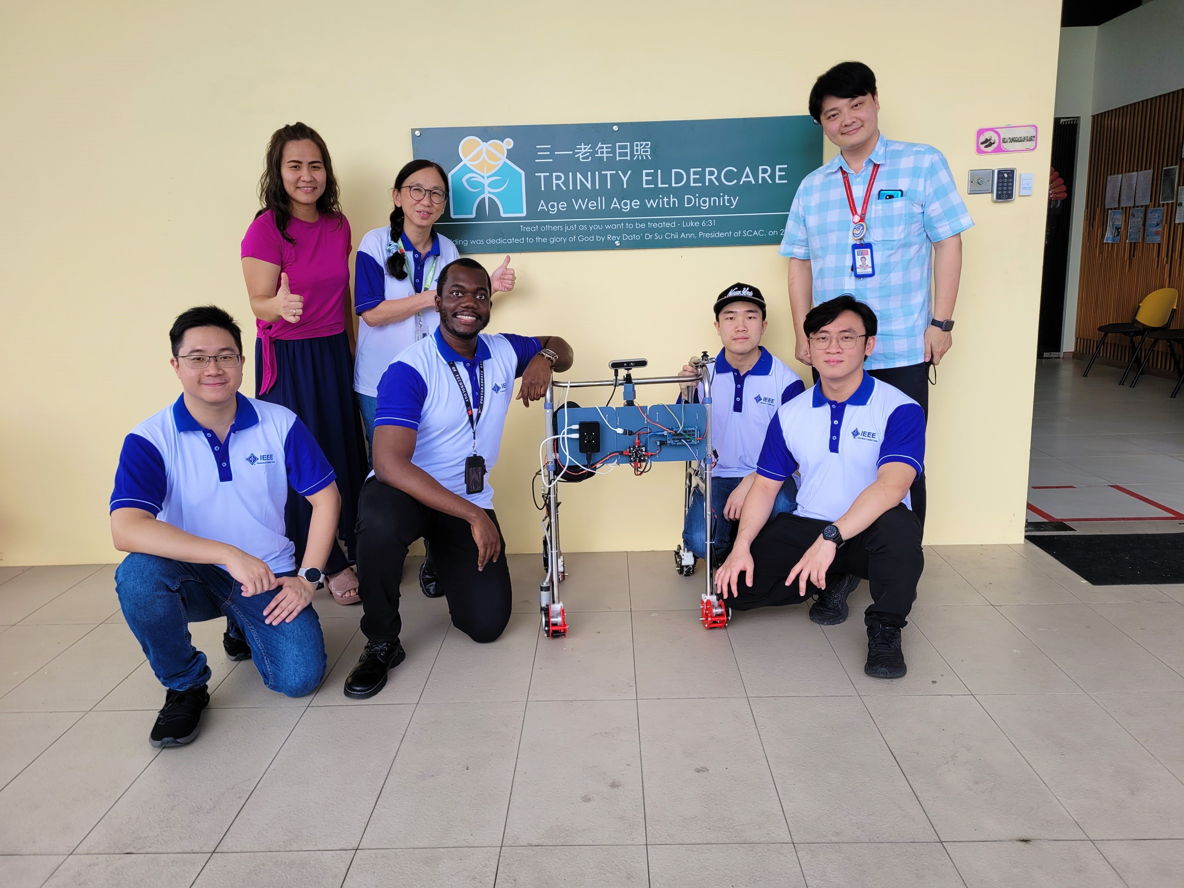

 Gary MarcusBen Wong


 While Nvidia has several types of GPUs deployed, the big guns found in data centers are the H100 and H200. As soon as the end of 2024, they will be joined by the B200, which nearly quadruples the H100’s performance on a per-GPU basis.Sources: Nvidia, MLPerf inferencing v4.1 results for Llama2-70B
 David Plunkert


 John Logie Baird [shown here] used the heads of ventriloquist dummies in early experiments because they didn’t mind the heat and bright lights of his televisor. Science History Images/Alamy
 The inset on the left shows how the televisor split an image (in this case, a person’s face) into vertical lines. Bettmann/Getty Images
 In 1926, Baird loaned part of the televisor he used in his Selfridges demo to the Science Museum in London.PA Images/Getty Images


 Rami SinnoAWS
 Ali SaidiAWS


 Today’s filters screen out unwanted RF signals by converting them to ultrasonic signals and back again. New research could lead to a way to integrate many such filters onto a single chip.NTT Corporation

 IEEE Fellow Grace Hopper inputting call numbers into the Universal Automatic (UNIVAC I), which allows the computer to find the correct instructions to complete. The A-0 compiler translates the English instructions into machine-readable binary code.Computer History Museum

 Khalifa University will be hosting IROS 2024 to highlight the Middle East and North Africa (MENA) region’s rapidly advancing capabilities in the robotics and intelligent transport systems.Khalifa University
 Khalifa University’s Center for Robotics and Autonomous Systems (KU-CARS) includes a vibrant multidisciplinary environment for conducting robotics and autonomous vehicle-related research and innovation.Khalifa University


 A cathode coating is deposited for R&D battery cells by Forge Nano.Forge Nano


 The AI scientist is an end-to-end scientific discovery tool powered by large language models. University of British Columbia


 Moriah Hargrove Anders
 Siemens Canada
 Vermont Electric Power Company and Shana Louiselle

