Reading view

There are new articles available, click to refresh the page.

A Match Made in Yorktown Heights


It pays to have friends in fascinating places. You need look no further than the cover of this issue and the article “ IBM’s Big Bet on the Quantum-Centric Supercomputer” for evidence. The article by Ryan Mandelbaum, Antonio D. Córcoles, and Jay Gambetta came to us courtesy of the article’s illustrator, the inimitable graphic artist Carl De Torres, a longtime IEEE Spectrum contributor as well as a design and communications consultant for IBM Research.

Story ideas typically originate with Spectrum’s editors and pitches from expert authors and freelance journalists. So we were intrigued when De Torres approached Spectrum about doing an article on IBM Research’s cutting-edge work on quantum-centric supercomputing.

De Torres has been collaborating with IBM in a variety of capacities since 2009, when, while at Wired magazine creating infographics, he was asked by the ad agency Ogilvy to work on Big Blue’s advertising campaign “Let’s build a Smarter Planet.” That project went so well that De Torres struck out on his own the next year. His relationship with IBM expanded, as did his engagements with other media, such as Spectrum, Fortune, and The New York Times. “My interest in IBM quickly grew beyond helping them in a marketing capacity,” says De Torres, who owns and leads the design studio Optics Lab in Berkeley, Calif. “What I really wanted to do is get to the source of some of the smartest work happening in technology, and that was IBM Research.”

Last year, while working on visualizations of a quantum-centric supercomputer with Jay Gambetta, vice president and lead scientist of IBM Quantum at the Thomas J. Watson Research Center in Yorktown Heights, N.Y., De Torres was inspired to contact Spectrum’s creative director, Mark Montgomery, with an idea.

“I really loved this process because I got to bring together two of my favorite clients to create something really special.” —Carl De Torres

“I thought, ‘You know, I think IEEE Spectrum would love to see this work,’” De Torres told me. “So with Jay’s permission, I gave Mark a 30-second pitch. Mark liked it and ran it by the editors, and they said that it sounded very promising.” De Torres, members of the IBM Quantum team, and Spectrum editors had a call to brainstorm what the article could be. “From there everything quickly fell into place, and I worked with Spectrum and the IBM Quantum team on a visual approach to the story,” De Torres says.

As for the text, we knew it would take a deft editorial hand to help the authors explain what amounts to the peanut butter and chocolate of advanced computing. Fortunately for us, and for you, dear reader, Associate Editor Dina Genkina has a doctorate in atomic physics, in the subfield of quantum simulation. As Genkina explained to me, that speciality is “adjacent to quantum computing, but not quite the same—it’s more like the analog version of QC that’s not computationally complete.”

Genkina was thrilled to work with De Torres to make the technical illustrations both accurate and edifying. Spectrum prides itself on its tech illustrations, which De Torres notes are increasingly rare in the space-constrained era of mobile-media consumption.

“Working with Carl was so exciting,” Genkina says. “It was really his vision that made the article happen, and the scope of his ambition for the story was at times a bit terrifying. But it’s the kind of story where the illustrations make it come to life.”

De Torres was happy with the collaboration, too. “I really loved this process because I got to bring together two of my favorite clients to create something really special.”

This article appears in the September 2024 print issue.

Atomically Thin Materials Significantly Shrink Qubits


Quantum computing is a devilishly complex technology, with many technical hurdles impacting its development. Of these challenges two critical issues stand out: miniaturization and qubit quality.

IBM has adopted the superconducting qubit road map of reaching a 1,121-qubit processor by 2023, leading to the expectation that 1,000 qubits with today’s qubit form factor is feasible. However, current approaches will require very large chips (50 millimeters on a side, or larger) at the scale of small wafers, or the use of chiplets on multichip modules. While this approach will work, the aim is to attain a better path toward scalability.

Now researchers at MIT have been able to both reduce the size of the qubits and done so in a way that reduces the interference that occurs between neighboring qubits. The MIT researchers have increased the number of superconducting qubits that can be added onto a device by a factor of 100.

“We are addressing both qubit miniaturization and quality,” said William Oliver, the director for the Center for Quantum Engineering at MIT. “Unlike conventional transistor scaling, where only the number really matters, for qubits, large numbers are not sufficient, they must also be high-performance. Sacrificing performance for qubit number is not a useful trade in quantum computing. They must go hand in hand.”

The key to this big increase in qubit density and reduction of interference comes down to the use of two-dimensional materials, in particular the 2D insulator hexagonal boron nitride (hBN). The MIT researchers demonstrated that a few atomic monolayers of hBN can be stacked to form the insulator in the capacitors of a superconducting qubit.

Just like other capacitors, the capacitors in these superconducting circuits take the form of a sandwich in which an insulator material is sandwiched between two metal plates. The big difference for these capacitors is that the superconducting circuits can operate only at extremely low temperatures—less than 0.02 degrees above absolute zero (-273.15 °C).

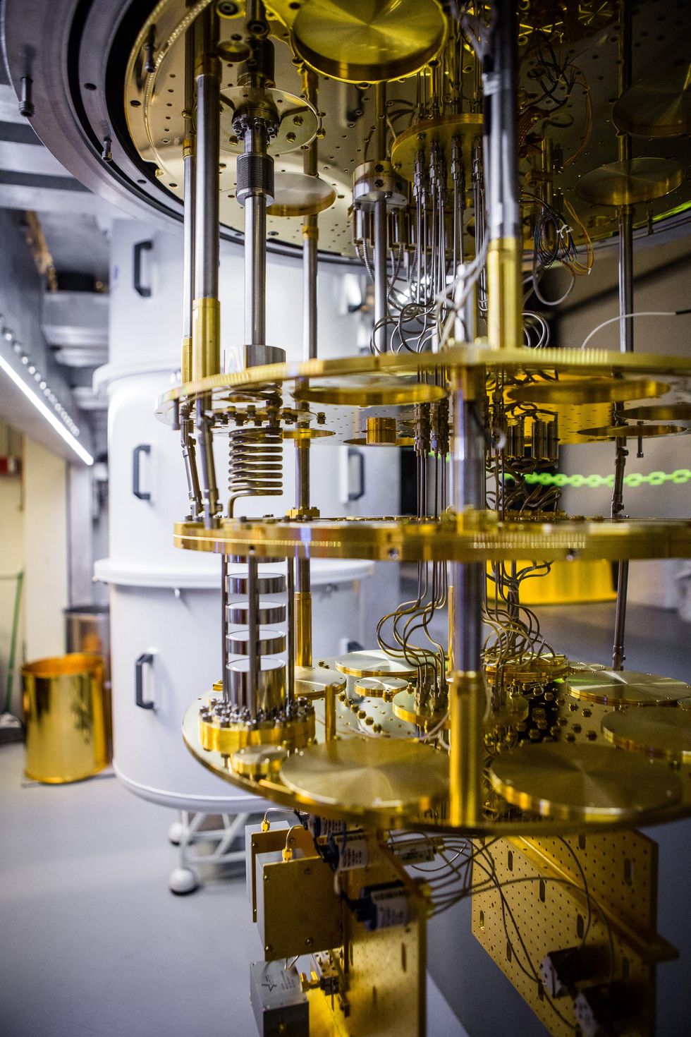
Golden dilution refrigerator hanging vertically Superconducting qubits are measured at temperatures as low as 20 millikelvin in a dilution refrigerator.Nathan Fiske/MIT

In that environment, insulating materials that are available for the job, such as PE-CVD silicon oxide or silicon nitride, have quite a few defects that are too lossy for quantum computing applications. To get around these material shortcomings, most superconducting circuits use what are called coplanar capacitors. In these capacitors, the plates are positioned laterally to one another, rather than on top of one another.

As a result, the intrinsic silicon substrate below the plates and to a smaller degree the vacuum above the plates serve as the capacitor dielectric. Intrinsic silicon is chemically pure and therefore has few defects, and the large size dilutes the electric field at the plate interfaces, all of which leads to a low-loss capacitor. The lateral size of each plate in this open-face design ends up being quite large (typically 100 by 100 micrometers) in order to achieve the required capacitance.

In an effort to move away from the large lateral configuration, the MIT researchers embarked on a search for an insulator that has very few defects and is compatible with superconducting capacitor plates.

“We chose to study hBN because it is the most widely used insulator in 2D material research due to its cleanliness and chemical inertness,” said colead author Joel Wang, a research scientist in the Engineering Quantum Systems group of the MIT Research Laboratory for Electronics.

On either side of the hBN, the MIT researchers used the 2D superconducting material, niobium diselenide. One of the trickiest aspects of fabricating the capacitors was working with the niobium diselenide, which oxidizes in seconds when exposed to air, according to Wang. This necessitates that the assembly of the capacitor occur in a glove box filled with argon gas.

While this would seemingly complicate the scaling up of the production of these capacitors, Wang doesn’t regard this as a limiting factor.

“What determines the quality factor of the capacitor are the two interfaces between the two materials,” said Wang. “Once the sandwich is made, the two interfaces are “sealed” and we don’t see any noticeable degradation over time when exposed to the atmosphere.”

This lack of degradation is because around 90 percent of the electric field is contained within the sandwich structure, so the oxidation of the outer surface of the niobium diselenide does not play a significant role anymore. This ultimately makes the capacitor footprint much smaller, and it accounts for the reduction in cross talk between the neighboring qubits.

“The main challenge for scaling up the fabrication will be the wafer-scale growth of hBN and 2D superconductors like [niobium diselenide], and how one can do wafer-scale stacking of these films,” added Wang.

Wang believes that this research has shown 2D hBN to be a good insulator candidate for superconducting qubits. He says that the groundwork the MIT team has done will serve as a road map for using other hybrid 2D materials to build superconducting circuits.

❌